

Optical semiconductor light emitting device, lighting apparatus, and display device
a light emitting device and optical semiconductor technology, applied in the direction of semiconductor devices, basic electric elements, electrical appliances, etc., can solve the problems of reducing the reduction of the light emitted from the optical semiconductor light emitting element, and the luminance of the optical semiconductor light emitting device. , to achieve the effect of enhancing the luminance, reducing the emission of blue light components, and enhancing the color rendering properties
- Summary
- Abstract
- Description
- Claims
- Application Information
AI Technical Summary
Benefits of technology
Problems solved by technology
Method used
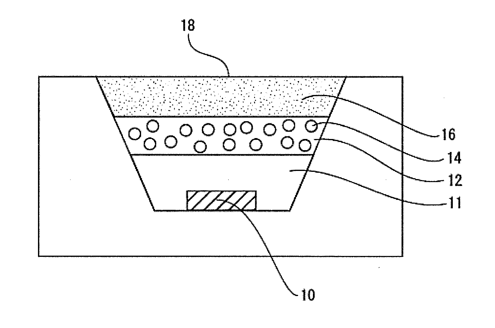
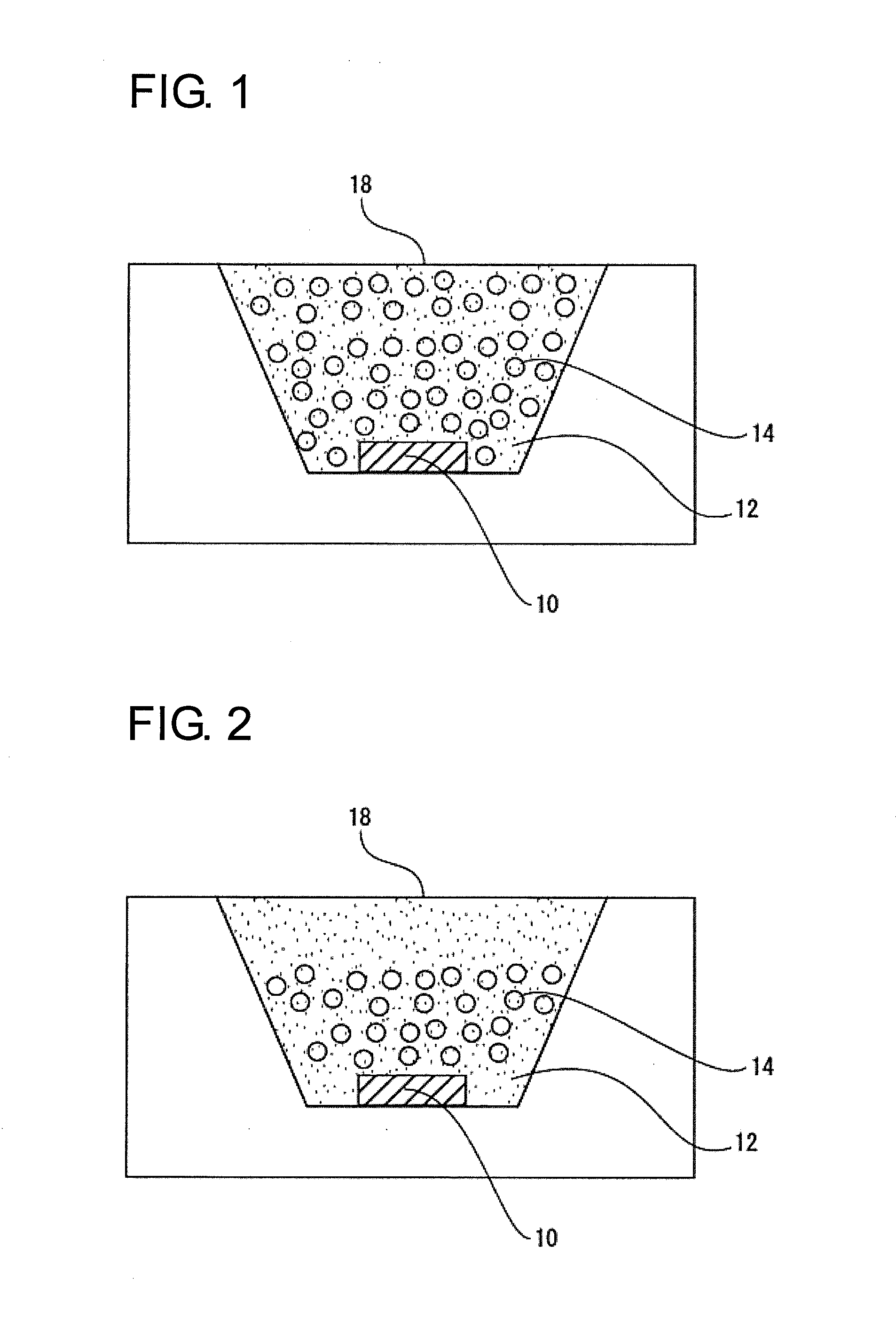
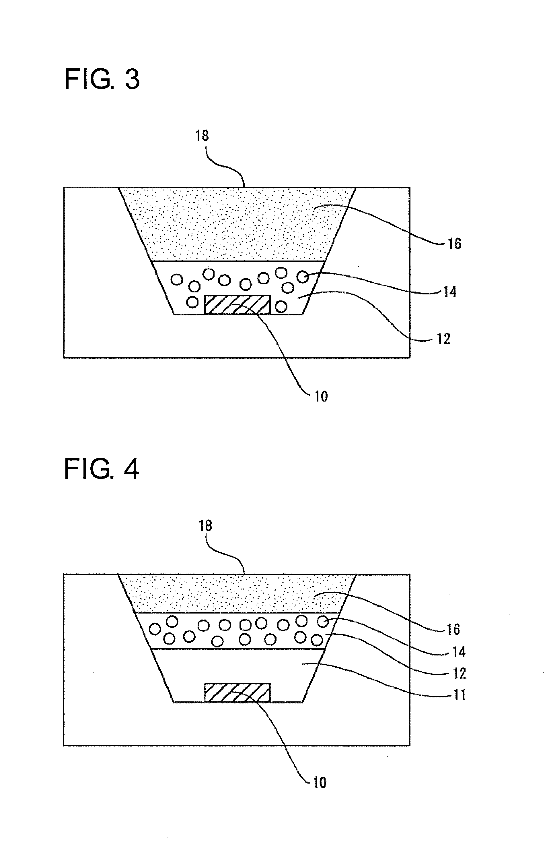
Image

Examples
example 1
Manufacture of Zirconia Particle
[0056]Dilute ammonia water obtained by dissolving 344 g of 28% ammonia water in 20 L of pure water was added to a zirconium salt solution obtained by dissolving 2615 g of zirconium oxychloride octahydrate in 40 L (liters) of pure water while being stirred, thereby preparing a zirconia precursor slurry.
[0057]An aqueous solution of sodium sulfate obtained by dissolving 300 g of sodium sulfate in 5 L of pure water was added to the slurry while being stirred, thereby obtaining a mixture. The amount of sodium sulfate added at this time was 30% by mass with respect to the equivalent zirconia value of zirconium ions in the zirconium salt solution.
[0058]The mixture was dried in the air at 130° C. for 24 hours by using a dryer, thereby obtaining a solid. The solid was crushed by an automatic mortar, and was then baked in the air at 520° C. for 1 hour by using an electric furnace.
[0059]Subsequently, the baked product was inserted into pure water and was stirred...
example 2
[0064]Zirconia particles having an average primary particle size of 7.8 nm were manufactured in the same manner as in Example 1 except that a temperature of 520° C. in the air set by the electric furnace during the manufacture of the zirconia particles was changed to 550° C. During the preparation of a surface modifying zirconia dispersion, vinyltrimethoxysilane of Example 1 was changed to methyldichlorosilane (LS-50 manufactured by Shin-Etsu Chemical Co, Ltd.) as an H—Si group-containing modifying material, and after heating and stirring were performed at 50° C. for 3 hours, a modifying and dispersing treatment was performed thereon under reflux at 130° C. for 3 hours, thereby preparing a zirconia transparent dispersion. The surface modification amount achieved by the H—Si group-containing surface modifying material was 40% by mass with respect to the mass of the zirconia particles. A light scattering composition and an optical semiconductor light emitting device were manufactured ...
example 3
[0065]Zirconium particles having an average primary particle size of 5.5 nm were manufactured in the same manner as in Example 1. During the preparation of a surface modifying zirconia dispersion, vinyltrimethoxysilane of Example 1 was changed to tetraethoxysilane (KBE-04 manufactured by Shin-Etsu Chemical Co., Ltd.) as an alkoxy group-containing modifying material, and after heating and stirring were performed at 50° C. for 3 hours, a modifying and dispersing treatment was performed thereon under reflux at 130° C. for 3 hours, thereby preparing a zirconia transparent dispersion. The surface modification amount achieved by the alkoxy group-containing surface modifying material was 40% by mass with respect to the mass of the zirconia particles. During the preparation of a light scattering composition, 7.6 g of a condensation curing-type phenyl silicone resin (H62C manufactured by Wacker Asahikasei Silicone Co., Ltd.) was added to 50 g of the zirconia transparent dispersion and was st...
PUM
 Abstract
Description
Claims
Application Information