Flexible printed circuit board, planar light source apparatus, display apparatus, and electronic device

a printed circuit board and flexible technology, applied in the direction of sustainable manufacturing/processing, lighting support devices, final product manufacturing, etc., can solve the problems of insufficient bonding strength of the terminals, peeling or cracking of the solder, and the fillet of the solder is not formed, so as to maintain flexibility and high brightness

Inactive Publication Date: 2015-09-03
TOHOKU DENSHI CO LTD
View PDF7 Cites 2 Cited by
  • Summary
  • Abstract
  • Description
  • Claims
  • Application Information

AI Technical Summary

Benefits of technology

[0008]The terminals C of the LED chips 2 are installed on the lands L and are bonded with solder 3. Two LED chips 2 that are mounted adjacent to each other are electrically connected by the belt-shaped wire WL. The wire WL is covered and protected by the cover lay 12. Note that the cover lay 12 is machined using cutting or drilling, for example, and with a machining process, the width of the cover lay 12 covering the wire WL can be reduced to 0.3 mm. However, in general, the machining accuracy for the cover lay 12 is lower than the etching accuracy for the conductive foil according to which precise pattern formation is possible, and the like.
[0015]One or more embodiments of the present invention provides a technique according to which multiple electronic components that are to be connected to each other on a flexible printed circuit board can be mounted on the circuit board at a narrower pitch, with favorable solder fillets formed at the terminals of the electronic components.
[0017]With one or more embodiments of the present invention, the wire for electrically connecting the electronic components connects the lands in an indirect manner rather than connecting them in a straight line. For this reason, even if the interval between the two lands is narrow, it is possible to prevent a case in which molten solder flows across the wire from one land to the vicinity of another land when a terminal is soldered. For this reason, a separate configuration such as a cover lay does not need to be provided between the lands, and therefore the interval between the lands can be made smaller. According to one or more embodiments of the present invention, multiple electronic components that are to be connected to each other on a circuit board can be mounted thereon at a narrower pitch, with favorable solder fillets formed at the terminals of the electronic components.
[0019]According to one or more embodiments of the present invention, it is possible to further shorten the distance between the lands without being influenced by the machining accuracy of the cover lay while the strength of the flexible printed circuit board is maintained by the cover lay.
[0021]According to one or more embodiments of the present invention, since the wire exposed from the openings in the cover lay branches, it is easier to guide excessive molten solder from the lands to the wire. For this reason, it is possible to provide a flexible printed circuit board in which favorable fillets are easier to form at the terminals.
[0025]According to one or more embodiments of the present invention, it is possible to provide a flexible printed circuit board according to which light is emitted at a higher brightness while flexibility is maintained.

Problems solved by technology

However, in FIG. 2B, solder fillets are not formed.
Thus, if the solder fillets are not formed favorably at the terminals of the electronic components, there is a risk that the bond strength of the terminals will be insufficient.
In some cases, peeling or cracking of the solder occurs accompanying a load caused by bending or the like of the FPC, and the electronic components end up separating from the circuit board.

Method used


Image

  • Flexible printed circuit board, planar light source apparatus, display apparatus, and electronic device
  • Flexible printed circuit board, planar light source apparatus, display apparatus, and electronic device
  • Flexible printed circuit board, planar light source apparatus, display apparatus, and electronic device

Examples


embodiment 1

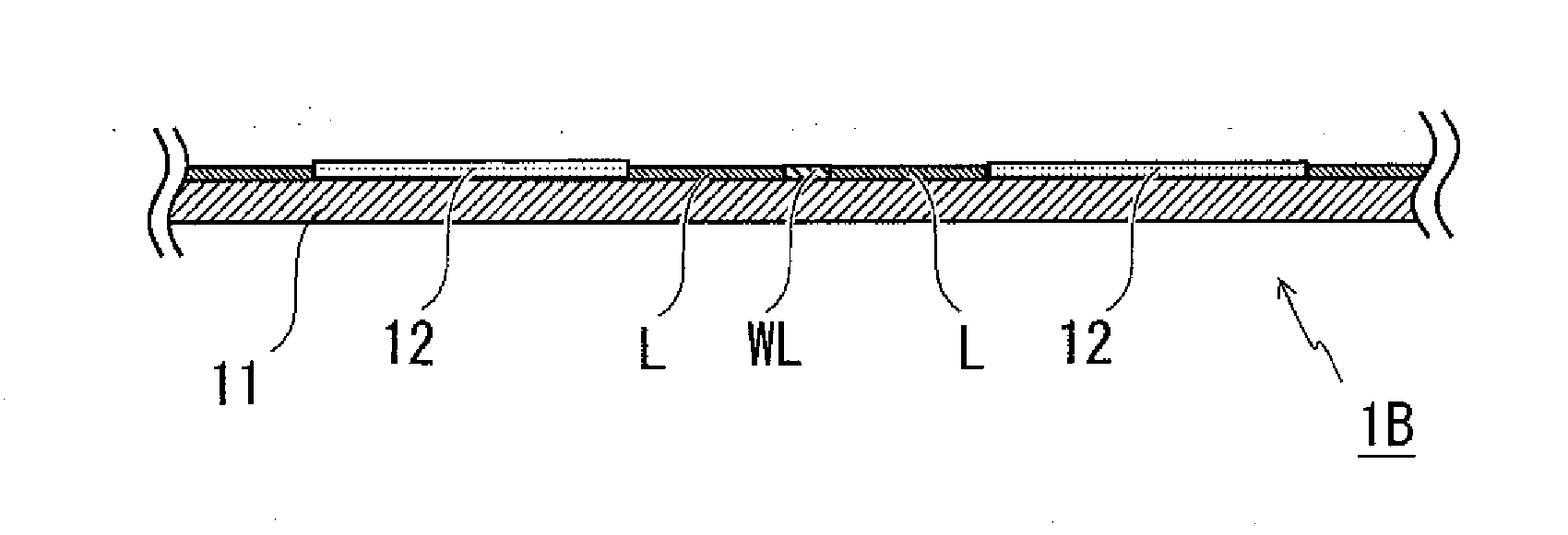
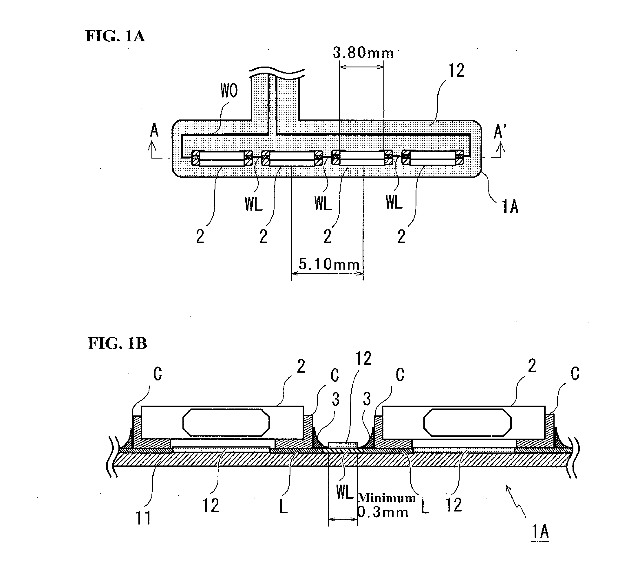
[0044]A description will be given in which an LED chip 2 mounted on a front surface is used as an electronic component according to Embodiment 1. Also, a description will be given in which a single-sided FPC is used as a flexible printed circuit board according to Embodiment 1. Note that the electronic component is not limited to being an LED chip 2, and may be a light-emitting electronic component other than an LED, an image sensor, or other electronic component, and it may be an electronic component that is connected by a lead. Also, the flexible printed circuit board may be what is referred to as a flexible printed wire board, a flexible wiring circuit board, or the like.

[0045]Overview of Configuration

[0046]FIGS. 3A to 3C are diagrams illustrating an FPC according to Embodiment 1. FIG. 3A is a plan view illustrating the front surface of an FPC 1. FIG. 3A shows the FPC 1 on which LED chips 21 to 24 are mounted linearly at a predetermined pitch. On the FPC 1 of Embodiment 1, 3.80-m...

embodiment 2

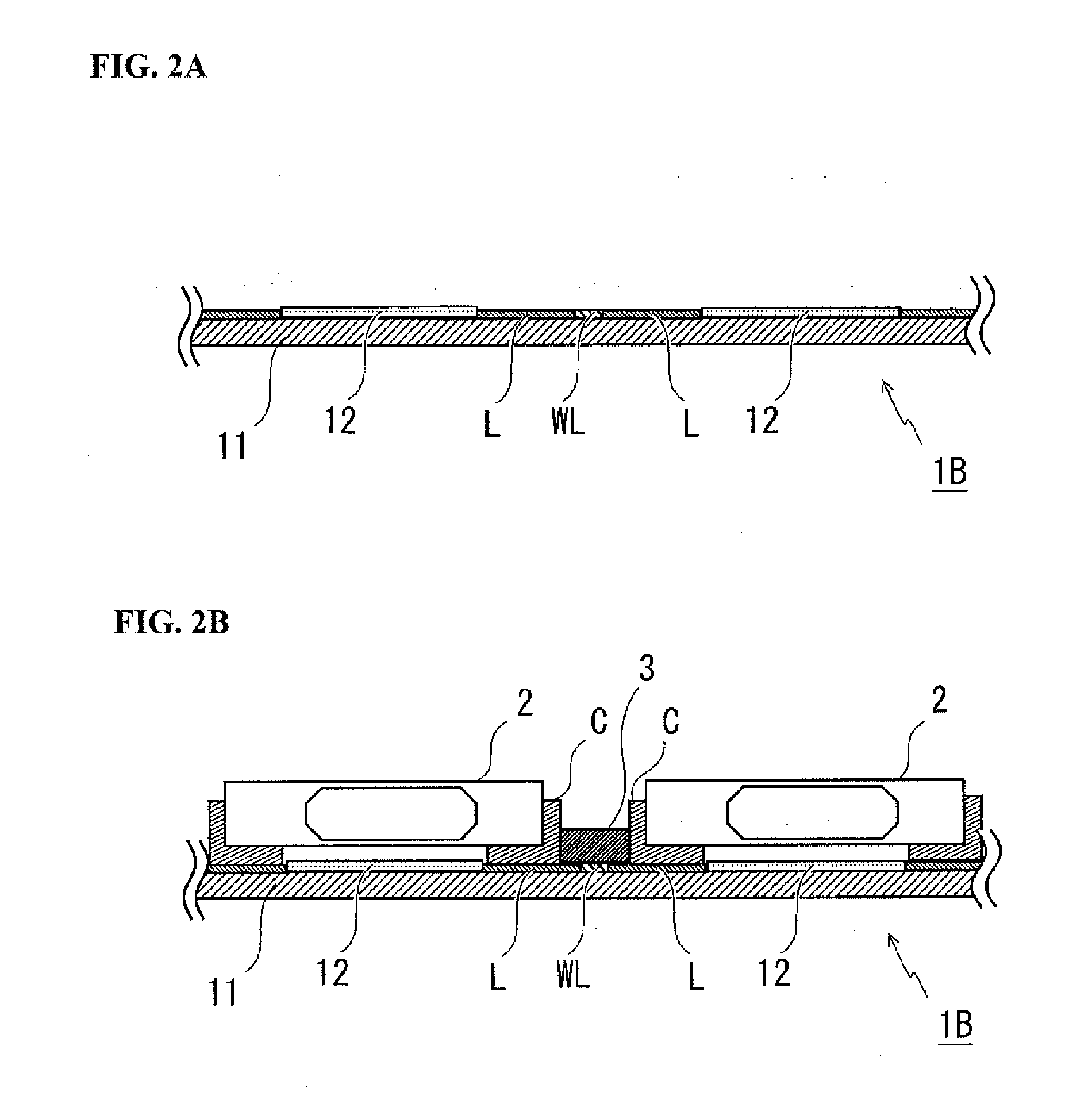
[0078]A description will be given in which a double-sided FPC on whose front surface the LED chips 2 are mounted is used as the flexible printed circuit board according to Embodiment 2. Note that an FPC having a structure with three or more layers may be used.

[0079]Similarly to the FPC 1 of Embodiment 1, multiple LED chips 2 are mounted linearly at a predetermined pitch on the front surface of the FPC of Embodiment 2. Wires between the LED chips 2 that are mounted adjacent to each other will be described next.

[0080]FIGS. 9A and 9B are diagrams illustrating wires between electronic components in the FPC according to Embodiment 2. FIGS. 9A and 9B show the vicinity of the cover lay opening portion N12 in an FPC 1′. FIG. 9A is a plan view showing the front surface of the FPC 1′. Two LED chips 2 can be mounted adjacent to each other in the vicinity of the cover lay opening portion N12. The land L1R, the land L2L, the inter-land wire WL12, and the base material 11 are exposed at the cover...


PUM


Abstract

A flexible printed circuit board on which a first electronic component and a second electronic component are to be mounted adjacent to each other has a first land for soldering a terminal of the first electronic component on a side adjacent to the second electronic component, and a second land for soldering a terminal of the second electronic component on a side adjacent to the first electronic component. The first land and the second land are connected by a wire extending outside of an inter-land region that is an approximately belt-shaped region formed by connecting end portions in a width direction or end portions in a thickness direction of the first land and the second land in a straight line.

Description

BACKGROUND[0001]1. Field[0002]The present invention relates to a flexible printed circuit board (referred to below as “FPC” as well) on which an electronic component is mounted.[0003]2. Related Art[0004]FPCs with superior thinness and flexibility are used in electronic devices that are smaller and thinner in order to use space efficiently. For example, an FPC on which LEDs (light emitting diodes) are mounted is used in a liquid crystal display as a light source for an edge-lit backlight using a light guide plate.[0005]JP 2003-101173A is an example of background art.SUMMARY[0006]FIGS. 1A and 1B are diagrams showing an example of a conventional FPC. FIGS. 1A and 1B show an FPC 1A on which multiple LED chips 2 are mounted, which is used as a light source for a backlight of a liquid crystal display apparatus. FIG. 1A is a plan view showing the front surface of the FPC 1A. With the FPC 1A, multiple LED chips 2 are mounted linearly and are connected by wires W0 and WL. A series circuit is...

Claims


Application Information

Patent Timeline
Patent Type & Authority Applications(United States)
IPC IPC(8): H05K1/02F21K99/00H05K1/11H01L27/15H01L33/62
CPCH05K1/028H01L27/15H01L33/62H05K1/0296F21Y2105/001F21K9/30H05K2201/10522F21Y2101/02H05K1/111H05K1/114H05K1/189H05K3/3442H05K2201/09254H05K2201/10106H05K2201/10136H05K2201/10287H05K2201/10295H05K2203/046Y02P70/50
Inventor NAMBU, KENSUKE
Owner TOHOKU DENSHI CO LTD
Why Eureka
Try Eureka