

Multilayer ceramic electronic component and assembly board having the same
- Summary
- Abstract
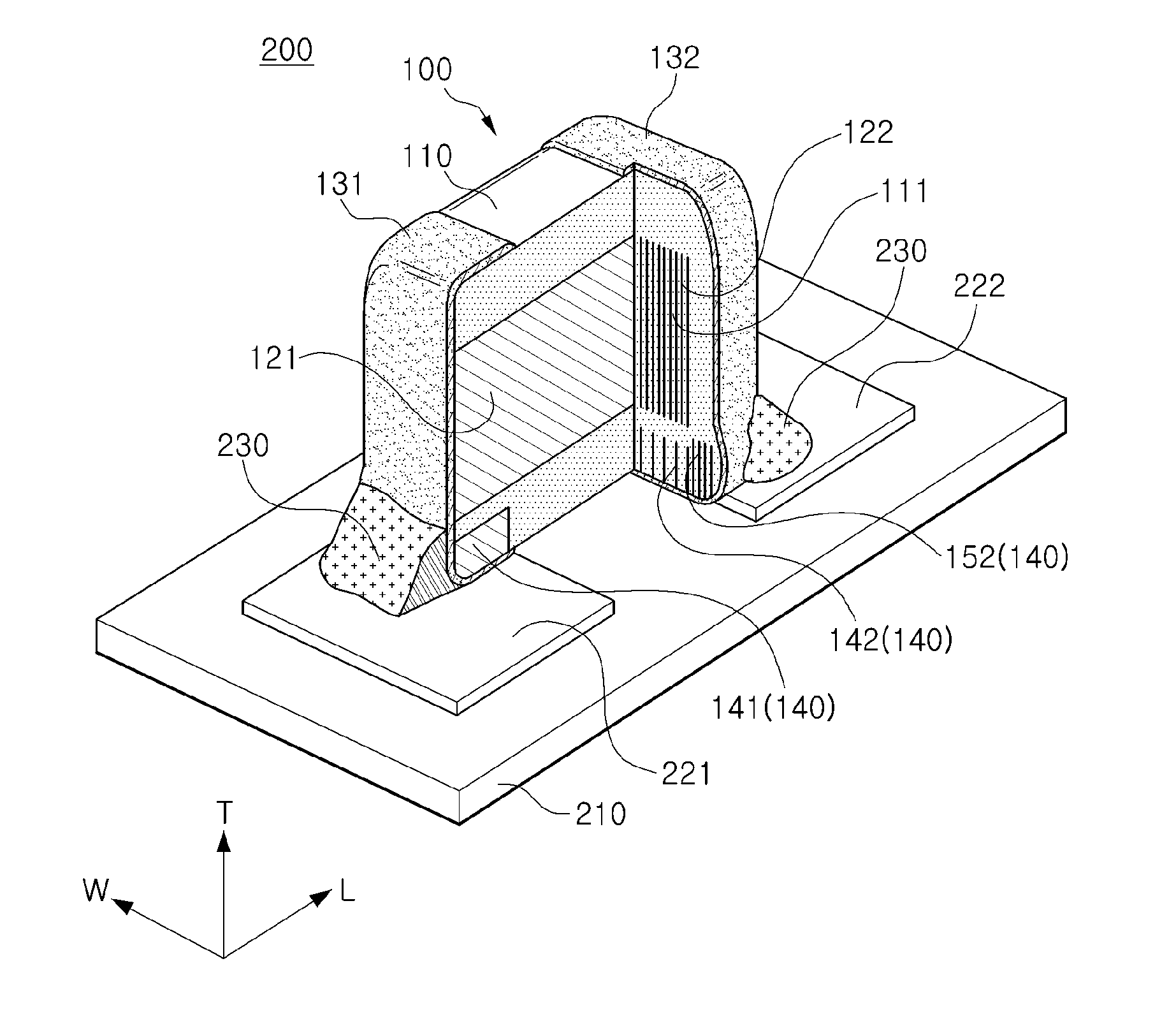
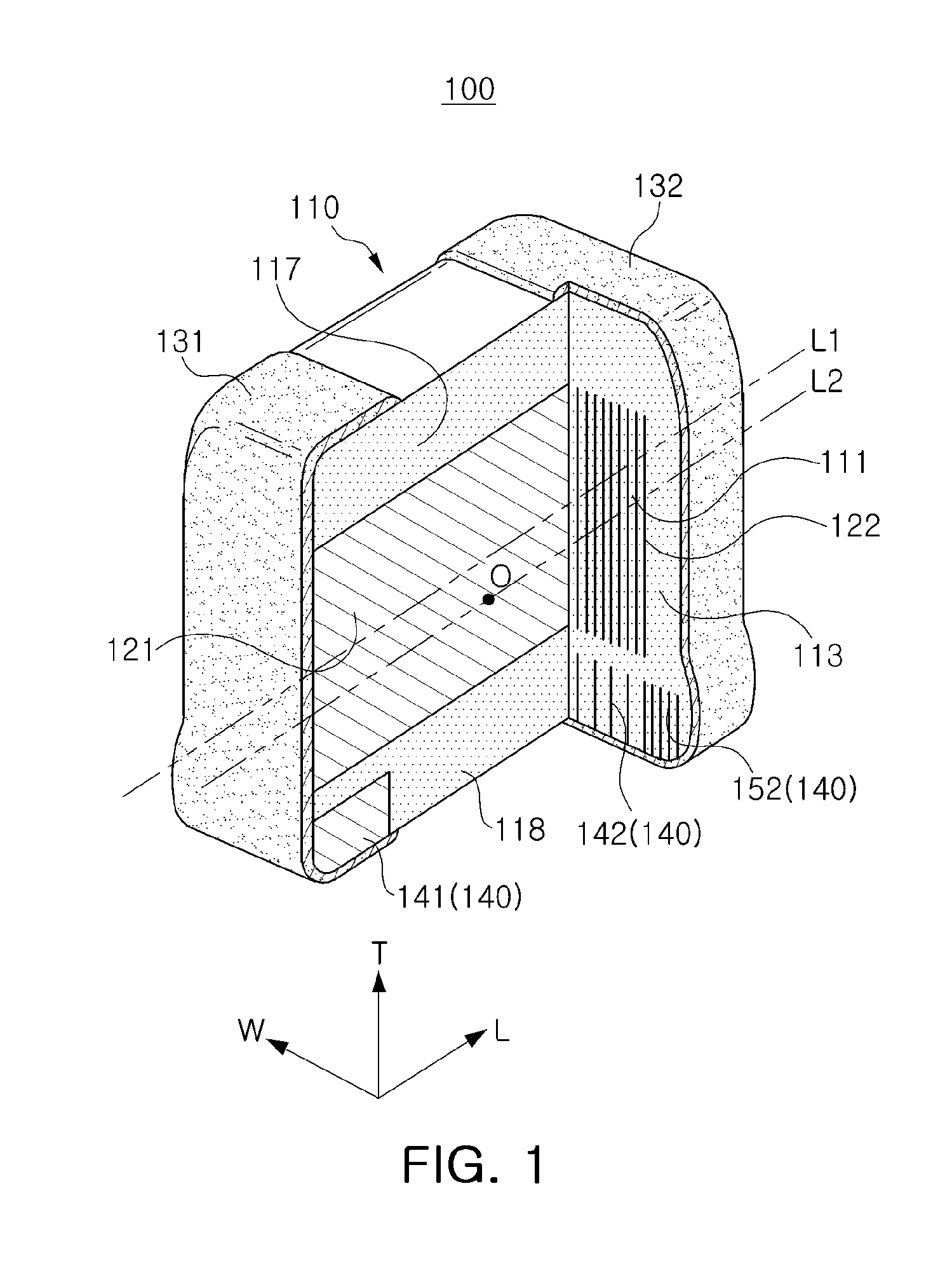
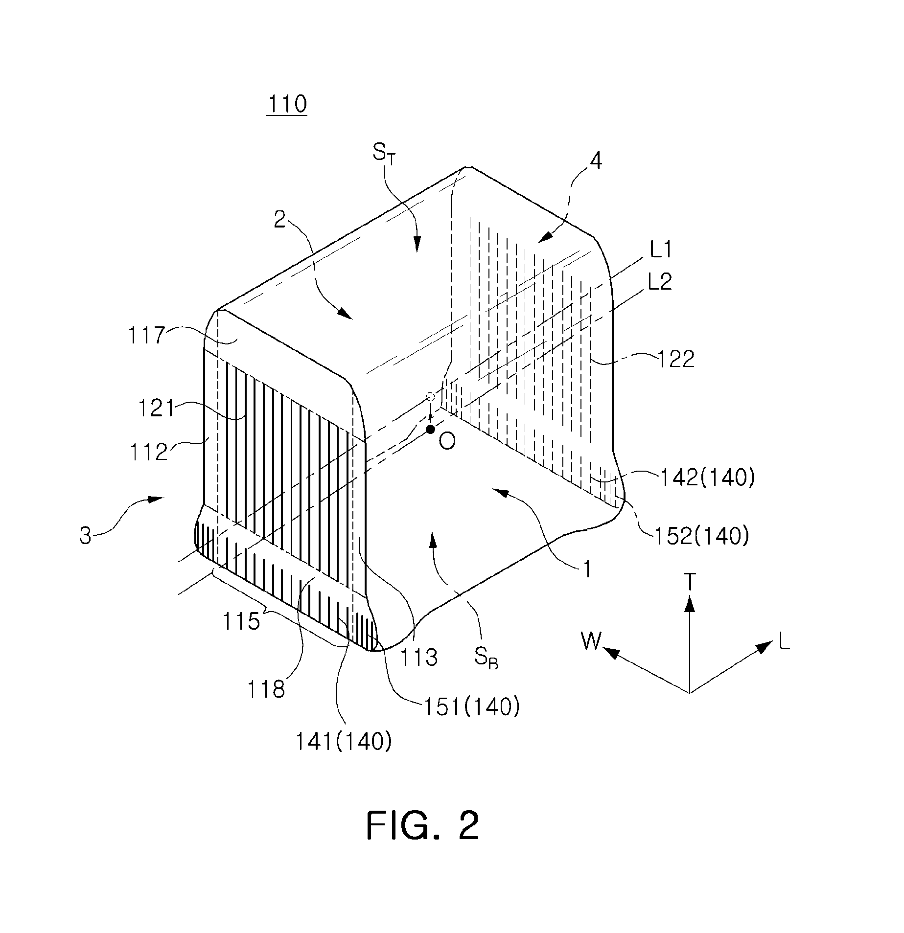
- Description
- Claims
- Application Information
AI Technical Summary
Benefits of technology
Problems solved by technology
Method used
Image

Examples
experimental examples
[0147]The following Table 1 illustrates results obtained by measuring frequencies of a pick-up defect and a mounting defect when multilayer ceramic electronic components of Comparative Examples and Inventive Examples are mounted on boards, in order to see if the frequencies of the defects are decreased since the multilayer ceramic electronic components according to Inventive Examples include a volume increasing part.
[0148]In the present Experimental Examples, a case in which a dummy electrode pattern part was only formed in a lower portion of an active part of a ceramic body in a thickness direction was set as Experimental Example 1; a case in which a dummy electrode pattern part was only formed in a lower portion of a cover part of a ceramic body in a thickness direction was set as Experimental Example 2; and a case in which a dummy electrode pattern part was formed in lower portions of active and cover parts of a ceramic body in a thickness direction was set as Experimental Exampl...
PUM
| Property | Measurement | Unit |
|---|---|---|
| Length | aaaaa | aaaaa |
| Thickness | aaaaa | aaaaa |
| Dielectric polarization enthalpy | aaaaa | aaaaa |
Abstract
Description
Claims
Application Information