Method for forming wiring

Active Publication Date: 2015-09-17
NANOBRIDGE SEMICON INC
View PDF3 Cites 35 Cited by
  • Summary
  • Abstract
  • Description
  • Claims
  • Application Information

AI Technical Summary

Benefits of technology

[0030]According to the present invention, it is possible to suppress the evolution of poisoning gas and to expose the prescribed wiring pattern by forming the multilayer resist structure on the semiconductor substrate, which includes the via hole, at a ti

Problems solved by technology

However, due to making the process temperature low, poisoning gas is evolved increasingly through a via hole, which is opened on an upper electrode of the BEOL device, in the via first dual damascene process, and a chemically amplification type material, which is included in an applied photo resist (PR), becomes inactive at a time of exposure for wiring after opening the via hole.
As a result, there is a problem that a resolution failure of wiring pattern is caused.
As a result, it becomes

Method used


Image

  • Method for forming wiring
  • Method for forming wiring
  • Method for forming wiring

Examples


first exemplary embodiment

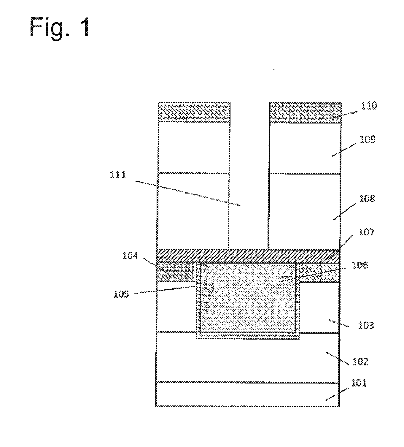
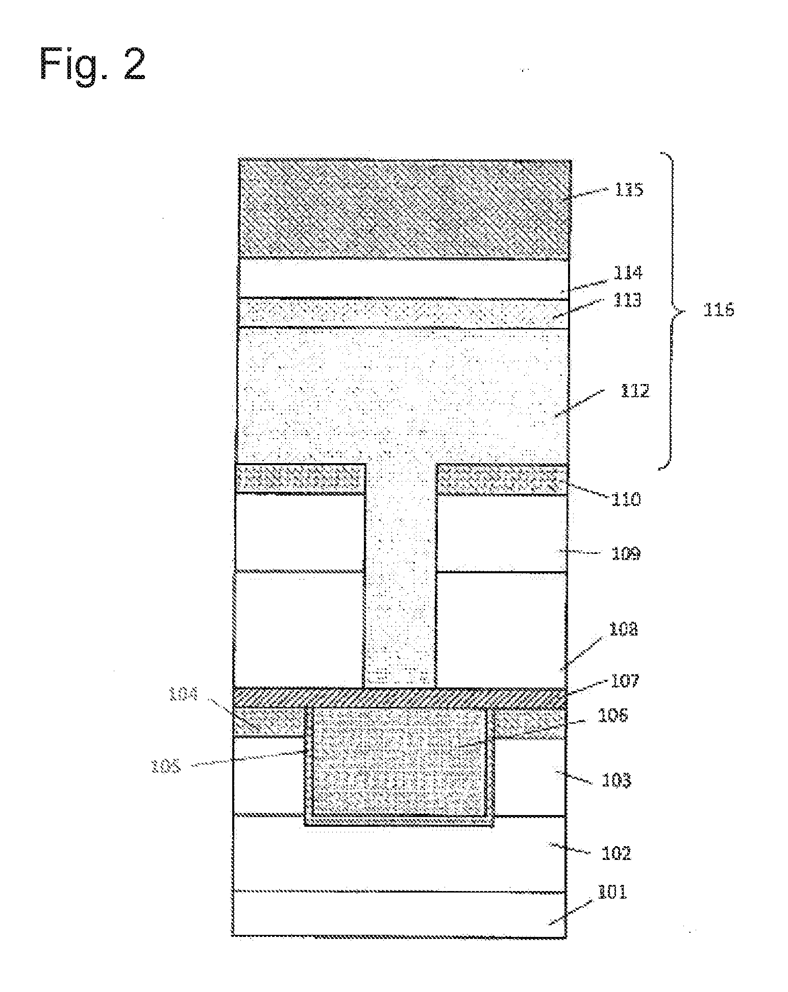
[0079]Each of FIG. 1 to FIG. 8 is a cross section for explaining a series of processes of: forming the via hole in a part of the interlayer insulating film, which is arranged on the semiconductor substrate, by carrying out the lithography and the dry etching; subsequently depositing the multilayer resist structure according to the present invention on the via hole; forming a desired wiring pattern by carrying out the lithography; and forming a copper wiring, which is connected with a lower layer wiring through the via, in the dual damascene process, out of processes for fabricating the copper wiring on the semiconductor substrate. Structure of the substrate, on which the copper wiring is formed, in the exemplary embodiment includes a semiconductor substrate 101, an interlayer insulating film 102, an interlayer insulating film 103, a cap insulating film 104, a barrier metal 105, a first wiring 106, a barrier insulating film 107 and a via hole 111. The semiconductor substrate 101 defi...

second exemplary embodiment

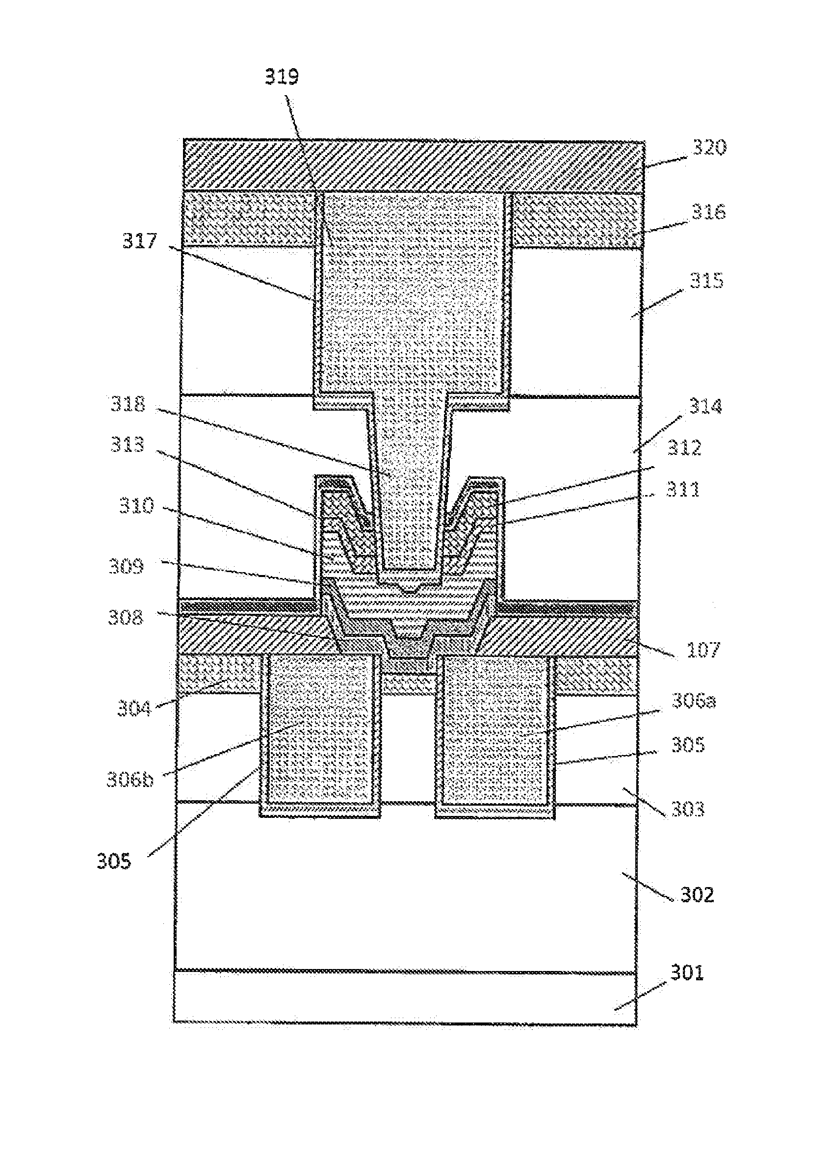
[0095]In a second exemplary embodiment which uses the wiring forming method of the present invention, a two-terminal-type solid electrolyte switch element, which is an example of the functional elements and which is formed in the multi-layered interconnection layer arranged on the semiconductor substrate, and a fabrication method thereof will be explained in the following with reference to FIGS. 9 to 24.

[0096]Firstly, operations of a resistance changing element and a solid electrolyte switch element, which is one of the resistance changing elements, will be explained briefly. FIG. 9 is a schematic diagram showing a cross section of the resistance changing element. The resistance changing element, which has three layers structure that a variable resistance layer 3 is interposed between a first electrode 1 (a lower electrode) and a second electrode 2 (an upper electrode), uses a phenomenon that a change in resistance is caused by applying a voltage between both electrodes. Each of FIG...

example

Example 1

[0150]After structure, which includes the via hole over the solid electrolyte switch element 124 as shown in FIG. 21, is formed, the wiring layer is formed correspondingly to each of the following three cases. That is, three cases includes a case of forming the multilayer resist structure comprising the SOC layer, the SOG layer, the high density SiO2 layer and the photo resist layer in this order from the substrate side according to the present invention, a case of forming the multilayer resist structure not including the high density SiO2 layer, and a case of forming the multilayer resist structure furthermore including a low density SiO2 layer, whose density is lower than 2.1 g / cm3, in place of the high density SiO2 layer. As a result on a yield of the solid electrolyte switch element which acquires the switching function by use of 3 V bias out of all of measured elements, a yield of 85.0% is acquired when using the low density SiO2 layer, and a yield of 79.1% is acquired...


PUM


Abstract

The present invention addresses the problem of inhibiting the evolution of a poisoning gas to eliminate wiring-pattern resolution failures and thereby forming a desired wiring layer structure to provide functional elements having an improved property yield. This method for forming multi-layered copper interconnect on a semiconductor substrate comprises: forming a multilayer resist structure to form a given resist pattern on a substrate including an interlayer dielectric film that has via holes which have been formed in part thereof and filled with an SOC layer, the multilayer resist structure comprising an SOC layer, an SOG layer, an SiO2 layer, and a chemical amplification type resist superposed in this order from the substrate side; conducting etching using the resist pattern as a mask to form a pattern for a wiring layer and via plugs; and forming the wiring layer and the via plugs in the pattern.

Description

TECHNICAL FIELD[0001]The present invention relates to a method for forming wiring.BACKGROUND ART[0002]Semiconductor devices, especially silicon devices, have been more highly integrated to achieve lower power consumption through miniaturization following the scaling law known as “Moore's Law”. Highly integrated devices have been developed so far at the pace of increasing the number of transistors in the devices four times every three years. In recent years, the gate length of a MOSFET is 20 nm or smaller. Because of rising costs for lithography processes, including costs of apparatus and mask set, and the physical limits such as operation limit and fluctuation limit of device scaling, there has been need for improvement in device performance through an approach other than the following scaling law.[0003]As a functional element which is formed inside a multi-layered copper interconnect on a semiconductor device, a variable resistance type non-volatile element (hereinafter, referred t...

Claims


Application Information

Patent Timeline
IPC IPC(8): H01L21/768H01L21/02
CPCH01L21/76802H01L21/76832H01L21/02164H01L21/02282H01L21/76879H01L21/31116H01L21/31122H01L21/31138H01L21/31144H01L21/76808H01L21/76814H01L2221/1036H01L21/02063H01L21/02126H01L21/02167H01L21/02274H01L21/32136H10N70/253H10N70/245H10N70/8416H10N70/883H10N70/063H10N70/826
Inventor OKAMOTO, KOICHIROTADA, MUNEHIROHADA, HIROMITSUSAKAMOTO, TOSHITSUGU
Owner NANOBRIDGE SEMICON INC
Why Eureka
Try Eureka