MEMS device and formation method thereof

a technology of microelectromechanical systems and sensors, applied in the direction of fluid pressure measurement, acceleration measurement using interia forces, instruments, etc., can solve the problems of complex fabrication process of existing mems devices having integrated multiple mems sensors, high cost, and low cost

Active Publication Date: 2015-10-01
SEMICON MFG INT (SHANGHAI) CORP
View PDF2 Cites 6 Cited by
  • Summary
  • Abstract
  • Description
  • Claims
  • Application Information

AI Technical Summary

Benefits of technology

[0009]One aspect of the present disclosure provides a method for forming a MEMS device. A substrate including integrated circuits therein is provided to form a first dielectric layer on the substrate. One or more first metal connections and second metal connections are formed in the first dielectric layer. The first metal connections and the second metal connections are electrically connected to the integrated circuits. A second dielectric layer is formed on the first dielectric layer. An acceleration sensor is formed in the second dielectric layer to electrically connect to the one or more first metal connections. One or more first metal vias are formed in the second dielectric layer to electrically connect to the second metal connections. A pressure sensor is formed on the second dielectric layer to electrically connect to the first metal vias.
[0034]The first electrode material layers 104 may be made of silicon germanium using a low temperature low pressure chemical vapor deposition (CVD) process. During the low temperature low pressure CVD process, damages to the integrated circuits in the substrate often resulted from a high temperature process may be avoided. The formed first electrode material layers 104 may have significantly low stress. Thus, when using the first electrode material layers 104 as portion of the fixed electrodes, large deformations resulted from large stress may be avoided, and the measuring accuracy of the acceleration sensor may be ensured.
[0009]One aspect of the present disclosure provides a method for forming a MEMS device. A substrate including integrated circuits therein is provided to form a first dielectric layer on the substrate. One or more first metal connections and second metal connections are formed in the first dielectric layer. The first metal connections and the second metal connections are electrically connected to the integrated circuits. A second dielectric layer is formed on the first dielectric layer. An acceleration sensor is formed in the second dielectric layer to electrically connect to the one or more first metal connections. One or more first metal vias are formed in the second dielectric layer to electrically connect to the second metal connections. A pressure sensor is formed on the second dielectric layer to electrically connect to the first metal vias.
[0035]The thickness of the first electrode material layers 104 may range approximately from 4500 angstroms to 5500 angstroms. The stress in the first dielectric material layers 104 may range approximately from −20 MPa to 20 MPa. The low temperature low pressure chemical vapor deposition (CVD) process used for forming the first electrode material layer 104 may use a silicon-containing source gas such as SiH4 or Si2H6, a germanium-containing source gas such as GeH2, a chamber temperature ranging approximately from 420° C. to 450° C., and a chamber pressure ranging approximately from 200 mTorr to 600 mTorr.
[0017]The present disclosure provides a MEMS device and formation method thereof. In an exemplary MEMS device formation method, by using a vertical integration approach, an acceleration sensor and a pressure sensor are formed on a substrate, and are electrically connected to integrated circuits formed in the substrate respectively. Integrated fabrication of the acceleration sensor and the pressure sensor is therefore realized. The pressure sensor is formed above the acceleration sensor, such that the pressure sensor and the acceleration sensor do not interfere with each other when in operation. Due to such integration, the overall volume of the formed MEMS device is significantly reduced.
[0010]Another aspect of the present disclosure provides a MEMS device. The MEMS device includes a substrate having integrated circuits therein. A first dielectric layer is located on the substrate. One or more first metal connections and second metal connections are formed in the first dielectric layer. The first metal connections and the second metal connections are electrically connected to the integrated circuits. A second dielectric layer is located on the first dielectric layer. An acceleration sensor is formed in the second dielectric layer and electrically connected to the one or more first metal connections. One or more first metal vias are located in the second dielectric layer, and electrically connected to the second metal connections. A pressure sensor is located on the second dielectric layer and electrically connected to the one or more first metal vias.

Problems solved by technology

However, because of great differences between various sensors in fabrication and packaging, to the date, there are no integrated MEMS sensor products on the market.
Consequently, existing MEMS devices having integrated multiple MEMS sensors may have complicated fabrication process and may be large in the volume with high cost.

Method used


Image

  • MEMS device and formation method thereof
  • MEMS device and formation method thereof
  • MEMS device and formation method thereof

Examples


Embodiment Construction

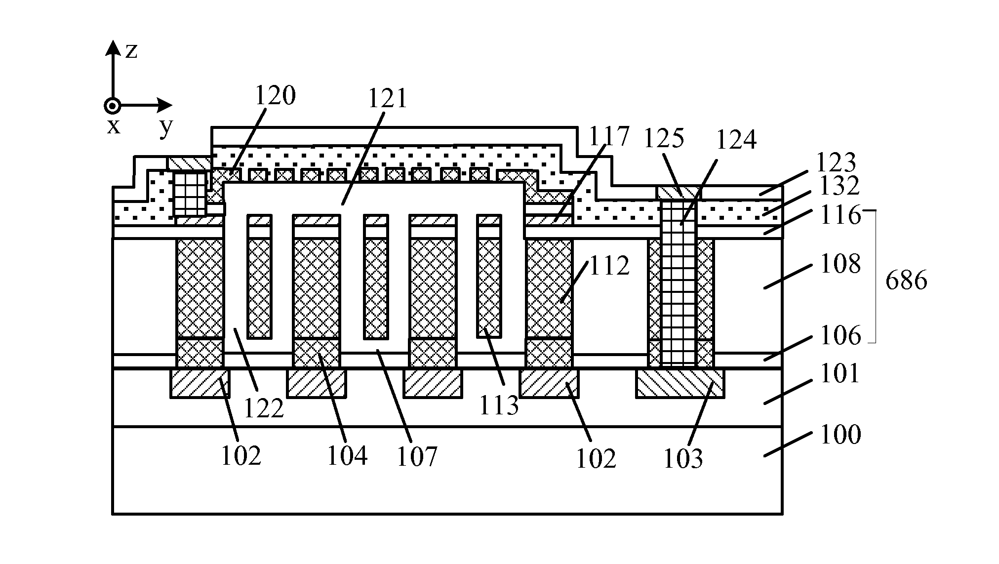
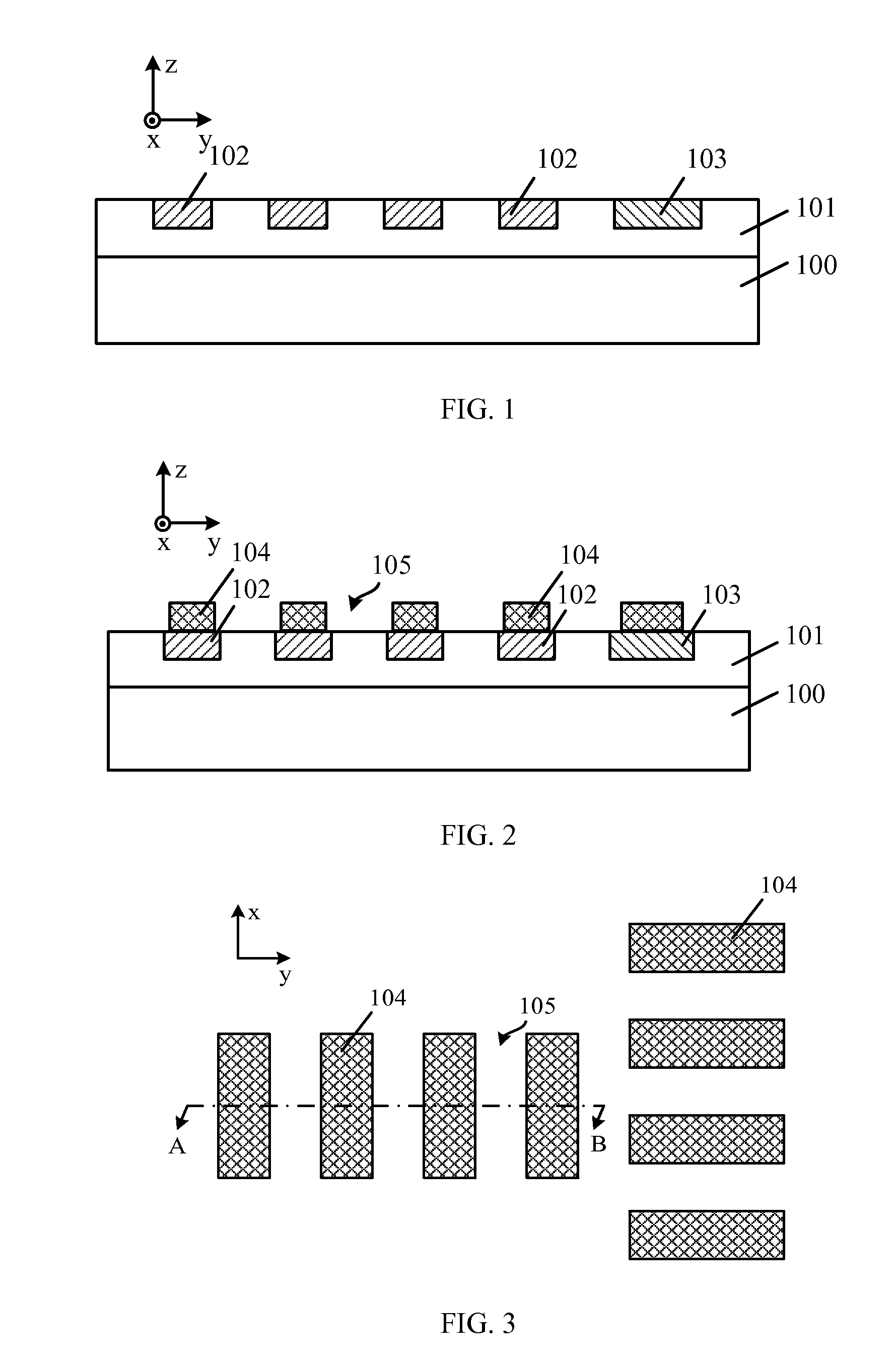
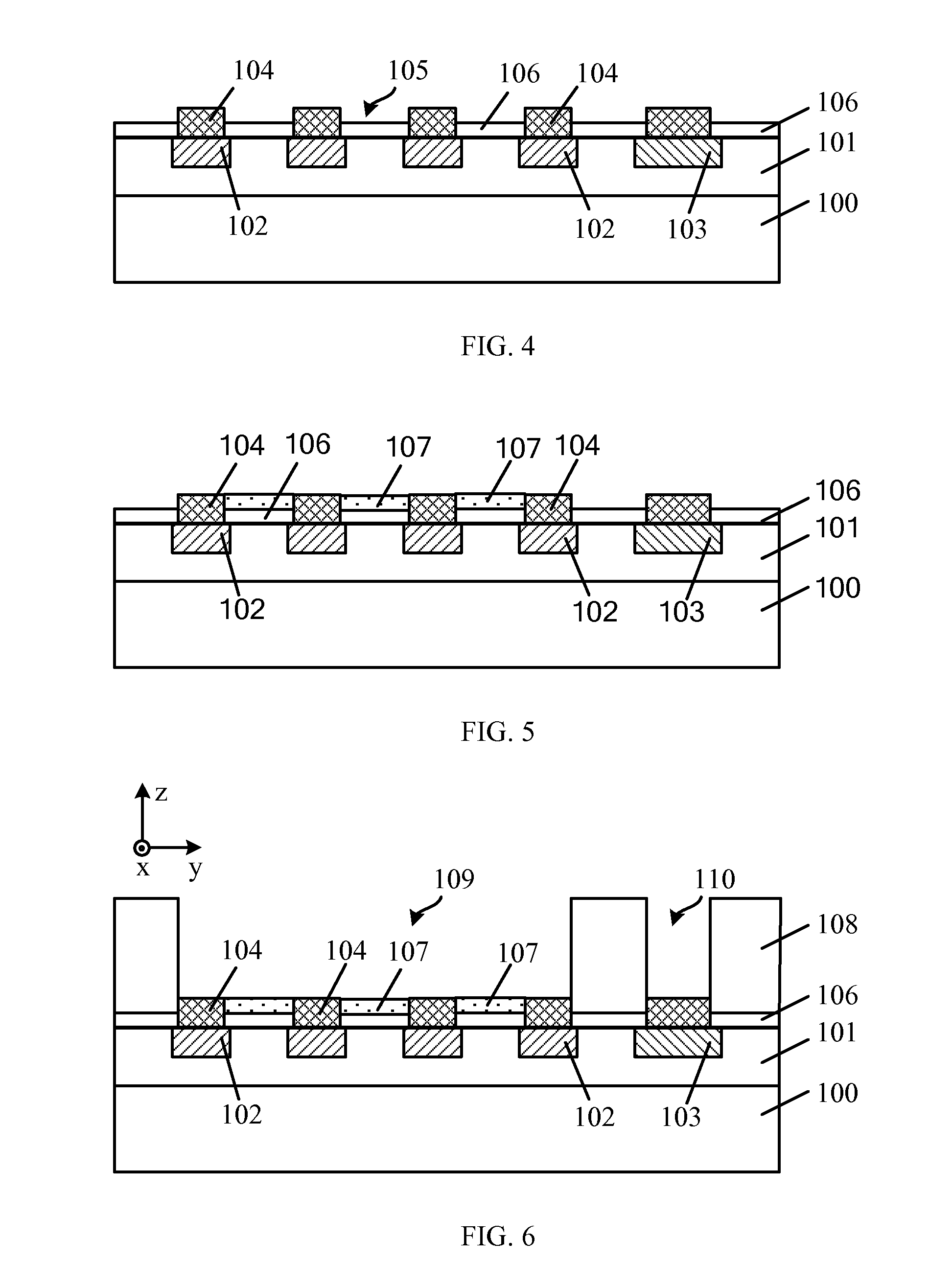
[0015]Reference will now be made in detail to exemplary embodiments of the invention, which are illustrated in the accompanying drawings. Hereinafter, embodiments consistent with the disclosure will be described with reference to drawings. Wherever possible, the same reference numbers will be used throughout the drawings to refer to the same or like parts. It is apparent that the described embodiments are some but not all of the embodiments of the present invention. Based on the disclosed embodiments, persons of ordinary skill in the art may derive other embodiments consistent with the present disclosure, all of which are within the scope of the present invention.

[0016]Fabrication processes of current MEMS acceleration sensors and MEMS pressure sensors are performed on different platforms, and the manufacturing cost is high. When packaging the acceleration sensors and the pressure sensors together to satisfy the requirements of particular applications, the packaged structure may hav...


PUM

PropertyMeasurementUnit
temperatureaaaaaaaaaa
chamber pressureaaaaaaaaaa
thicknessaaaaaaaaaa

Abstract

The present disclosure provides MEMS devices and their fabrication methods. A first dielectric layer is formed on a substrate including integrated circuits therein. One or more first metal connections and second metal connections are formed in the first dielectric layer and are electrically connected to the integrated circuits. A second dielectric layer is formed on the first dielectric layer. An acceleration sensor is formed in the second dielectric layer to electrically connect to the one or more first metal connections. One or more first metal vias are formed in the second dielectric layer to electrically connect to the second metal connections. A pressure sensor is formed on the second dielectric layer to electrically connect to the first metal vias. The MEMS devices provided by the present disclosure are compact in size through the integration of the acceleration sensor and the pressure sensor.

Description

CROSS-REFERENCES TO RELATED APPLICATIONS[0001]This application claims the priority of Chinese patent application No. CN201410113760.3, filed on Mar. 25, 2014, the entire content of which is incorporated herein by reference.FIELD OF THE DISCLOSURE[0002]The present disclosure relates to the field of Micro-Electro-Mechanical System (MEMS) technology and, more particularly, relates to a MEMS device and formation method thereof.BACKGROUND[0003]Micro-Electro-Mechanical System (MEMS) technology is a fast growing technology. In the MEMS technology, micro / nano sized materials / structures are designed, fabricated, measured, and controlled to be functional devices. Currently, MEMS devices in the market include acceleration sensors and pressure sensors.[0004]The MEMS acceleration sensors are devices utilizing the inertia property to perform the measurement. Based on sensing principles, the MEMS acceleration sensors can be categorized into different groups, including piezoresistive type, capaciti...

Claims


Application Information

Patent Timeline
Patent Type & Authority Applications(United States)
IPC IPC(8): B81B7/00B81C1/00
CPCB81B7/007B81C1/0038B81B7/02B81C2203/01B81B2201/0264B81B2207/07B81B2207/096B81B2201/0235G01P15/125G01L9/0042G01P15/0802
Inventor XU, WEILIU, GUOAN
Owner SEMICON MFG INT (SHANGHAI) CORP
Why Eureka
Try Eureka