

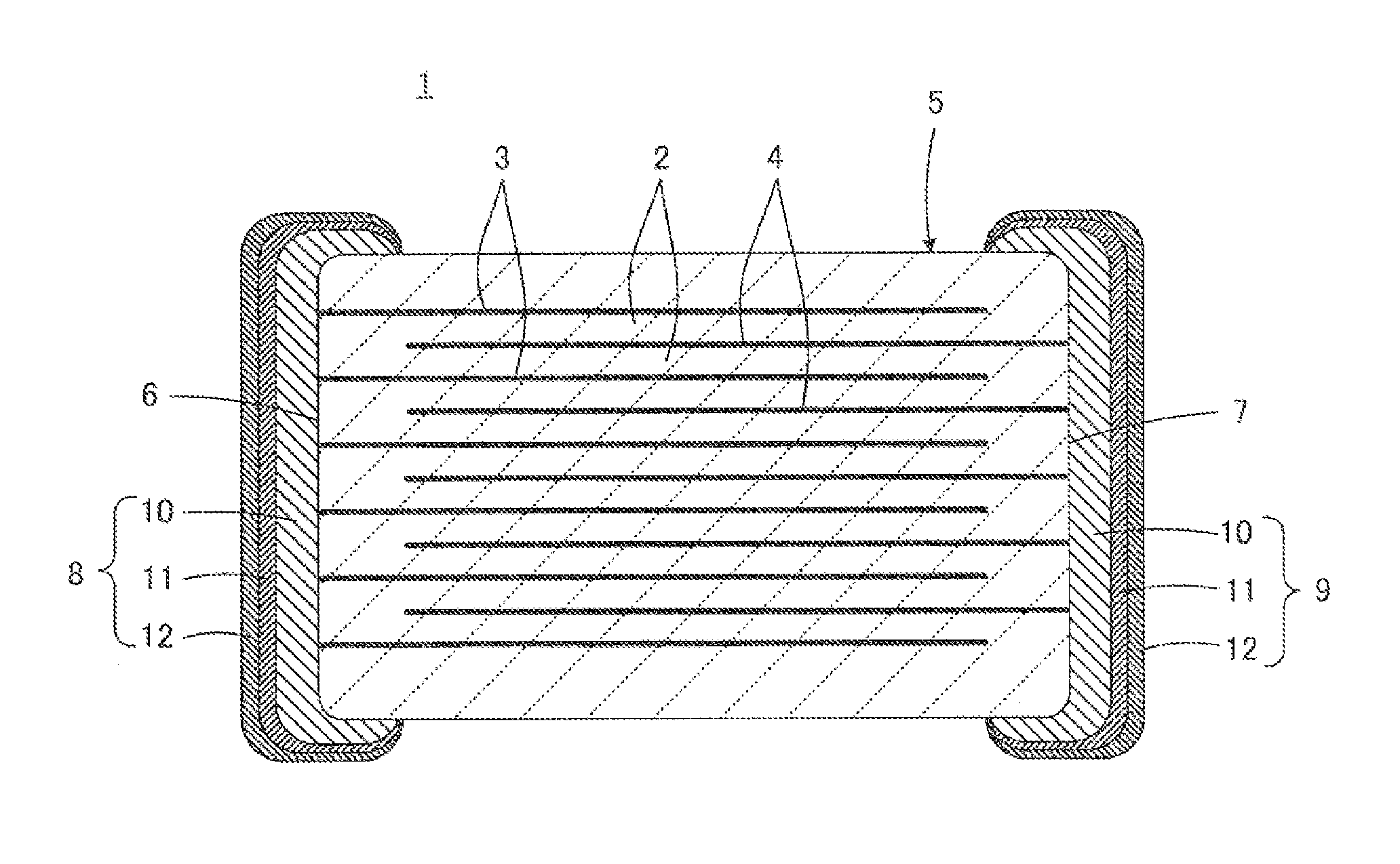
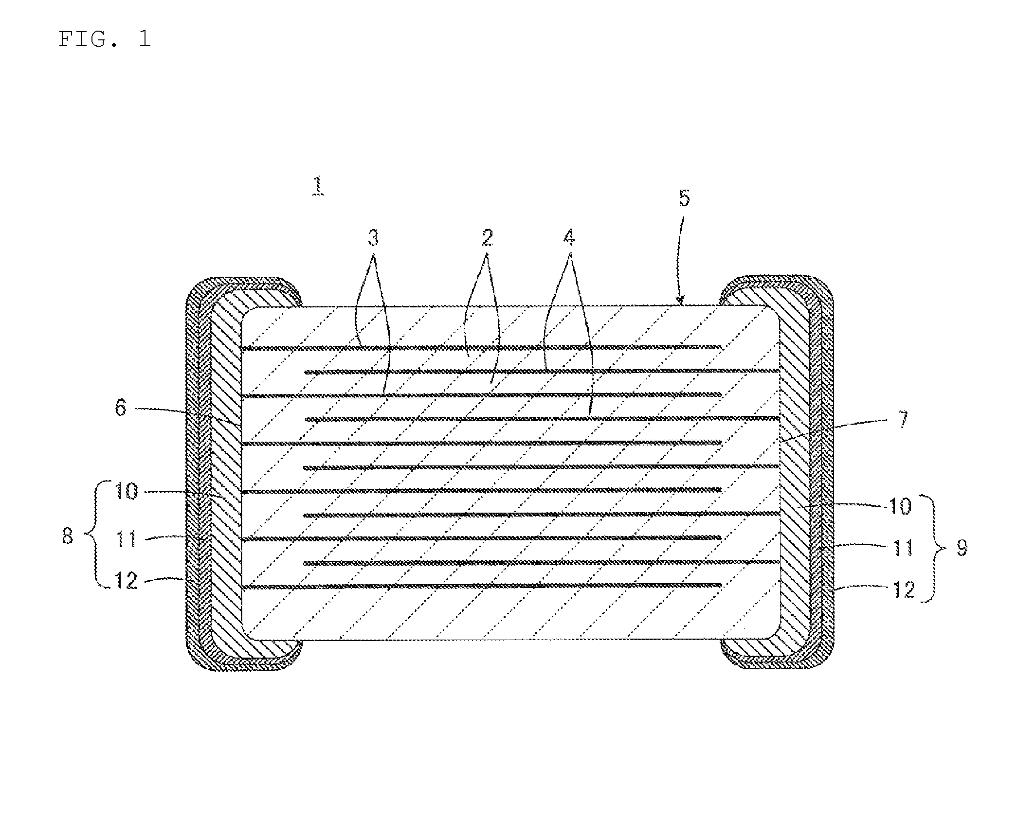
Laminated ceramic electronic component
a technology of electronic components and laminated ceramics, applied in the direction of fixed capacitors, stacked capacitors, fixed capacitor details, etc., can solve the problems of poor bondability of external electrodes to internal electrodes, and achieve satisfactory conductivity, satisfactory and stable electrical characteristics, and shrinkage amount of resin compositions during curing
- Summary
- Abstract
- Description
- Claims
- Application Information
AI Technical Summary
Benefits of technology
Problems solved by technology
Method used
Image

Examples
experimental example 1
Experimental Example of Changing Ratio of Sn
[0047](1) Preparation of Thermosetting Conductive Resin Composition
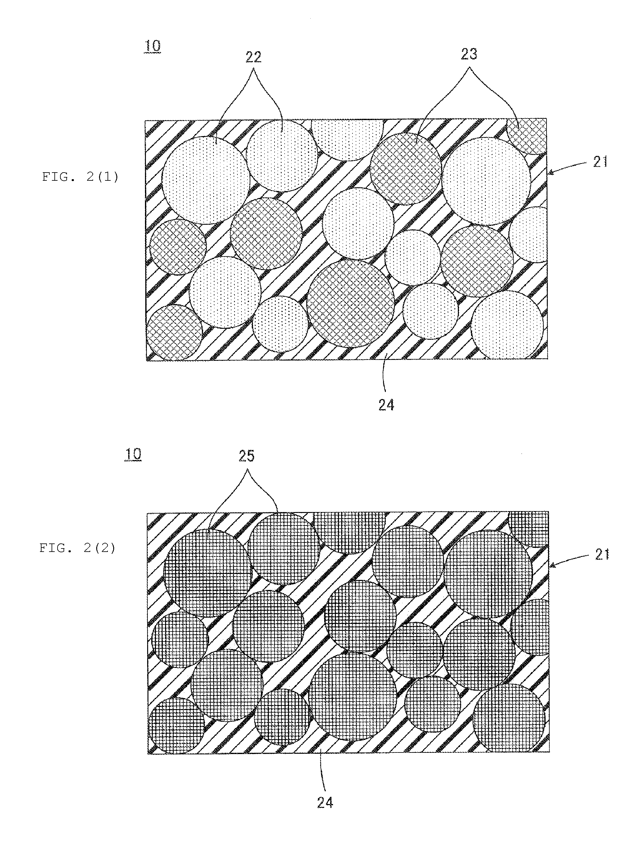
[0048]A Cu powder composed of spherical particles with a D50 value of 1.0 μm, a Sn powder composed of spherical particles with a D50 value of 2.5 μm, a resol-type phenolic resin A as a thermosetting resin and diethylene glycol monobutyl ether as an organic solvent were mixed by a small mixer, and then kneaded by metallic three rolls. Thereafter, the amount of diethylene glycol monobutyl ether as an organic solvent was adjusted while a viscosity was measured using an E-type viscometer, so that an uncured thermosetting conductive resin composition with the viscosity adjusted to 1 rpm / 30±2 Pa·s was obtained as a sample.
[0049]While the total content of the Cu powder and the Sn powder in the thermosetting conductive resin composition was 55% by volume after removal of the organic solvent, the ratio of Sn powder to the total amount of the Sn powder and the Cu powder was changed a...
experimental example 2
Experimental Example of Changing Ratio of Cu3Sn by Changing Conditions During Curing
[0105]Preparation of Thermosetting Conductive Resin Composition
[0106]A thermosetting conductive resin composition having a composition similar to sample 4 in Example 1.
[0107](2) Formation of Conducting Layer
[0108]Except that the top temperature and the keeping time during curing were changed as shown in the columns of “top temperature” and “keeping temperature”, respectively, in “curing” in Table 2, the same procedure as in Experimental Example 1 was carried out to obtain a laminated body in which a conducting layer in an external electrode was formed on each of both end surfaces.
[0109]The top temperature and the keeping time for obtaining sample 4-2 in Experimental Example 2 are identical, respectively, to the top temperature and the keeping time for obtaining sample 4 in Experimental Example 1.
[0110](3) Formation of Plating Layer
[0111]A laminated ceramic capacitor as a sample was obtained by formin...
experimental example 3
Experimental Example of Changing Thermosetting Resin
[0118]Preparation of Thermosetting Conductive Resin Composition
[0119]Except that the ratio of Sn powder to the total amount of the Sn powder and the Cu powder was fixed at 40% by weight and instead, as a thermosetting resin, one shown in the column of “type of thermosetting resin” in Table 3 was used, the same procedure as in Experimental Example 1 was carried out to obtain an uncured thermosetting conductive resin composition as a sample.
[0120](2) Formation of Conducting Layer
[0121]Under the same conditions as in Experimental Example 1, a thermosetting conductive resin composition was added to each of both end surfaces of a laminated body as a component main body for a laminated ceramic capacitor, and heat-treated to obtain a laminated body in which a conducting layer in an external electrode was formed on each of both end surfaces.
[0122](3) Formation of Plating Layer
[0123]A laminated ceramic capacitor as a sample was obtained by ...
PUM
| Property | Measurement | Unit |
|---|---|---|
| Fraction | aaaaa | aaaaa |
| Percent by mass | aaaaa | aaaaa |
| Percent by mass | aaaaa | aaaaa |
Abstract
Description
Claims
Application Information