
Optical modulation device

Active Publication Date: 2015-10-15
FUJIKURA LTD
View PDF2 Cites 34 Cited by
  • Summary
  • Abstract
  • Description
  • Claims
  • Application Information

AI Technical Summary

Benefits of technology

The invention aims to improve the efficiency of electrodes in devices by reducing the distance between the phase modulation unit and the device end portion. This reduces the loss of signal caused by the electrical properties of the electrode and the device. This results in improved modulation efficiency.

Problems solved by technology

According to this, a system necessary for optical communication is complicated, and thus problems such as an increase in a device size, an increase in the cost, and an increase in power consumption occur.
However, recently, optical communication using an optical fiber has been used due to demand for further increase in the speed and of further decreasing power consumption.
Furthermore, even in each level such as inside a board and inside the CPU of the computer, there is a problem in optical communication introduction.
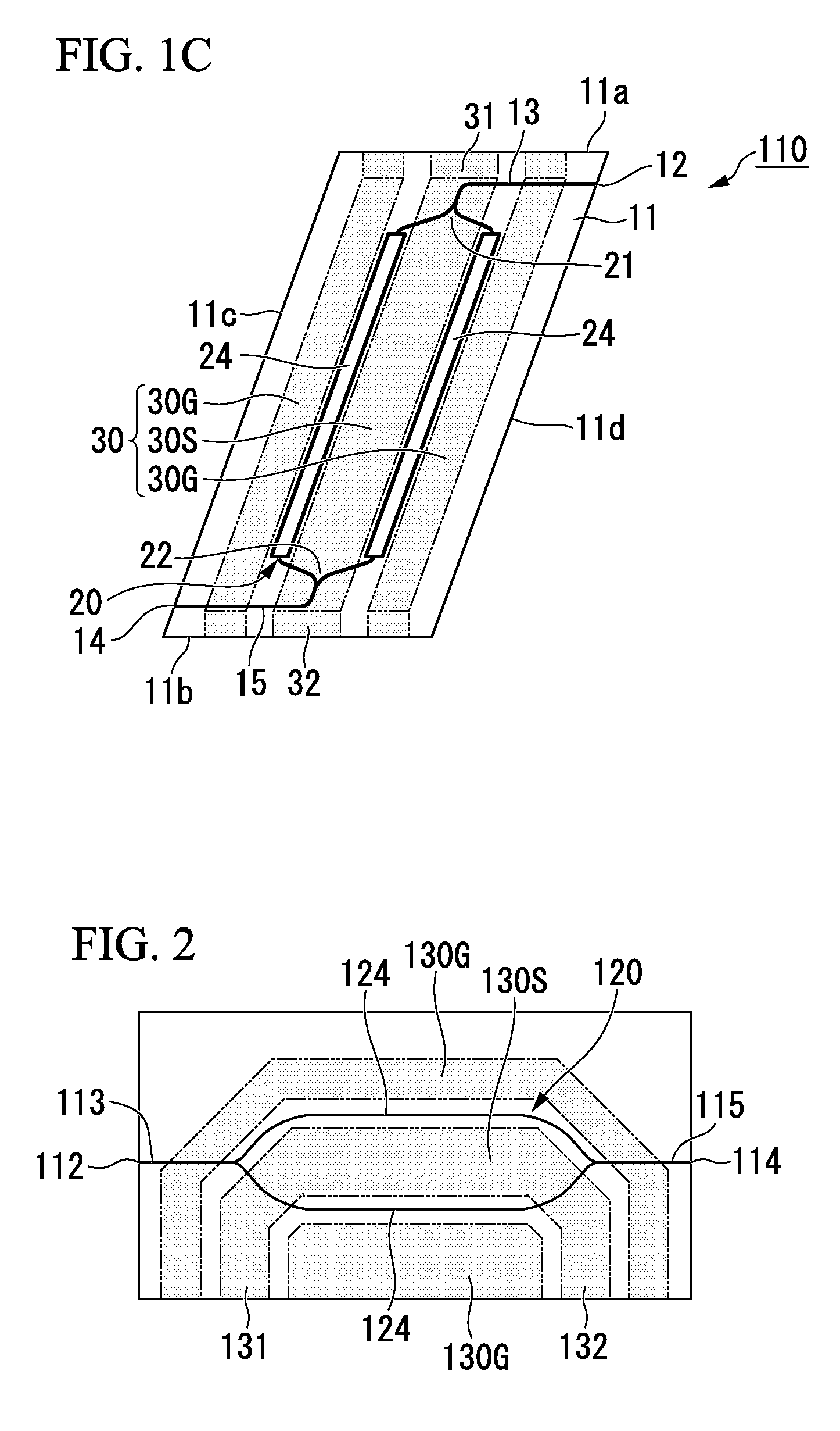
However, it is known that a traveling-wave electrode on a silicon substrate has a large propagation loss in the electrical signal, and when the electrode in a portion other than the phase modulation unit 124 is elongated, a loss due to a high frequency is remarkable in which modulation efficiency decreases due to a loss in power of the electrical signal, and thus a decrease in a modulation bandwidth is caused.

Method used


Image

  • Optical modulation device
  • Optical modulation device
  • Optical modulation device

Examples


first embodiment

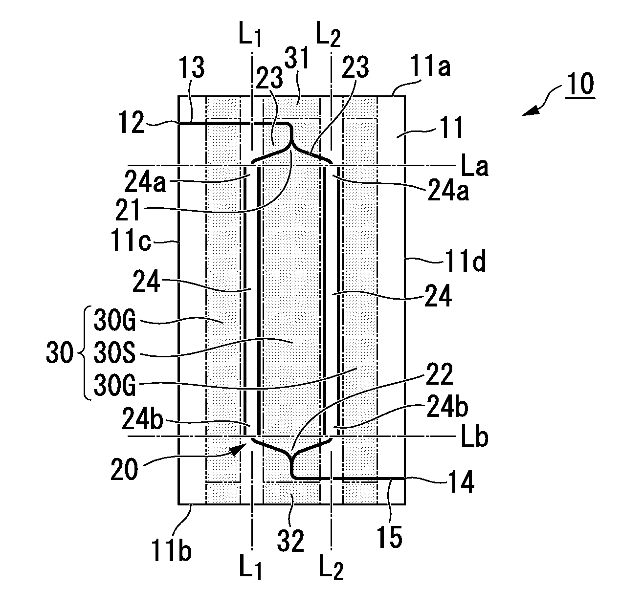
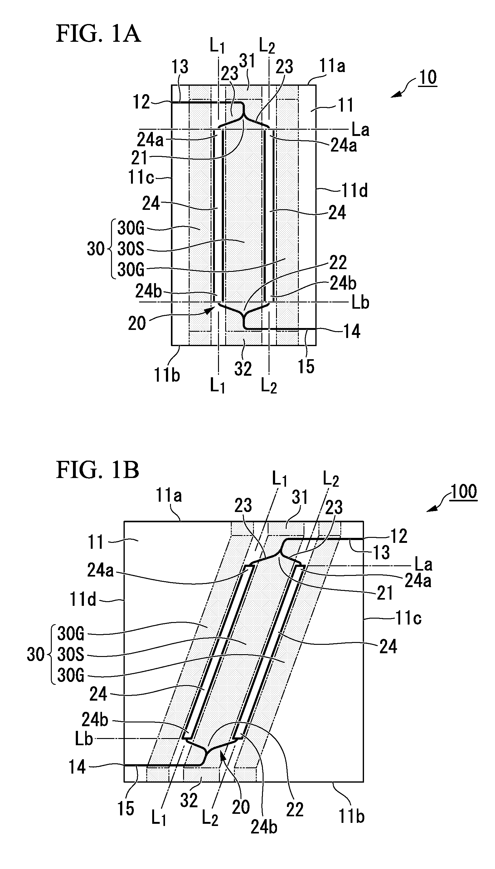
[0128]In FIGS. 1A to 1C, an optical modulation device of a first embodiment according to the present invention is illustrated. These optical modulation devices 10, 100, and 110 are configured of a planar optical waveguide 11 including a Mach-Zehnder interferometer 20. The Mach-Zehnder interferometer 20 includes two arm portions 23 between an optical splitter section (a first optical splitter section) 21 which branches one input light into two output lights, and an optical coupler section (a first optical coupler section) 22 which combines the light two input lights into one output light. Light which incident on the optical splitter section 21 from a light incidence unit 12 through an optical waveguide 13 is branched into the two arm portions 23 by the optical splitter section 21. After that, the branched lights are combined into one light by the optical coupler section 22 through the two arm portions 23, and the combined light is launched from the light launching unit 14 through an ...

second embodiment

[0152]In FIGS. 3A and 3B, an optical modulation device of a second embodiment according to the present invention is illustrated. Furthermore, in the following description, the same reference numerals are applied to the common configurations described above, and the repeated description thereof will be omitted.

[0153]Optical modulation devices 10A and 100A according to this embodiment are configured of the planar optical waveguide 11 including the Mach-Zehnder interferometer 20, as with the optical modulation devices 10, 100, and 110 of the first embodiment. In addition, in this embodiment, the light incidence unit 12 and the light launching unit 14 are positioned in a region between two lines La and Lb which extend in a direction in parallel with the two sides 11a and 11b from the two end portions 24a and 24b in the longitudinal direction of the phase modulation unit 24.

[0154]Here, the side on which the input unit 31 of the traveling-wave electrode 30 is arranged is defined as “11a”,...

third embodiment

[0164]In FIGS. 4A and 4B, an optical modulation device of a third embodiment according to the present invention is illustrated. Optical modulation devices 10B and 100B according to this embodiment are configured of the planar optical waveguide 11 including the Mach-Zehnder interferometer 20, as with the optical modulation devices 10 and 100 of the first embodiment. Furthermore, in the optical modulation device 10B of FIG. 4A, the longitudinal direction of the phase modulation unit 24 is perpendicular to the two sides 11a and 11b, but in the optical modulation device 100B of FIG. 4B, the longitudinal direction of the phase modulation unit 24 is inclined with respect to the two sides 11a and 11b.

[0165]In addition, in this embodiment, each of the arm portions 23 of the Mach-Zehnder interferometer 20 includes a phase adjustment unit (a second phase adjustment unit) 25 which is electrically independent and different from the phase modulation unit (the first phase adjustment unit) 24. Th...


PUM


Abstract

An optical modulation device configured of a planar optical waveguide, includes: a light incidence unit which allows light to be incident on the planar optical waveguide; a Mach-Zehnder interferometer which includes a first optical splitter section branching the light incident on the light incidence unit, two arm portions guiding the light branched by the first optical splitter section, a phase modulation unit linearly disposed on each of the two arm portions, and a first optical coupler section combining the light guided from the two arm portions; a light launching unit which launches the light combined by the first optical coupler section from the planar optical waveguide; and a traveling-wave electrode which includes an input unit and an output unit, and applies a voltage to the phase modulation unit.

Description

CROSS REFERENCE TO RELATED APPLICATIONS[0001]This application is a continuation application based on a PCT Patent Application No. PCT / JP2013 / 085137, filed Dec. 27, 2013, whose priority is claimed on Japanese Patent Application No. 2012-284723, filed on Dec. 27, 2012, and Japanese Patent Application No. 2012-284724, filed on Dec. 27, 2012BACKGROUND OF THE INVENTION[0002]1. Field of the Invention[0003]The present invention relates to a structure of an optical waveguide device which is manufactured on a substrate, and in particular, relates to the design of an electrode and a waveguide of an optical modulation device.[0004]2. Description of the Related Art[0005]Currently, the amount of information used in optical communication has been increasing. In order to respond to such an increase in the amount of information, a response such as an increase in a signal speed and an increase in the number of channels due to wavelength multiplexing communication has progressed in an optical communi...

Claims


Application Information

Patent Timeline
IPC IPC(8): G02F1/225G02B6/122G02F1/21G02B6/125
CPCG02F1/2257G02B6/125G02B6/1228G02F1/218G02F2001/212G02B2006/12159G02B2006/12097G02B2006/12147G02F1/2255G02F1/025G02B6/122G02B2006/12142G02F2201/58G02B6/29353G02B6/29355G02F1/212
Inventor GOI, KAZUHIROISHIHARA, HIROKIOGAWA, KENSUKEODA, KENJIKUSAKA, HIROYUKIMATSUMOTO, RYOKICHIUEMURA, HITOSHI
Owner FUJIKURA LTD
Learn More