Method of preparing a substrate for nanowire growth, and a method of fabricating an array of semiconductor nanostructures

a technology of nanowires and substrates, applied in the field of growth of semiconductor nanostructures, can solve the problems of difficult reproducibility of techniques and process that is actually non-positioned growth

Inactive Publication Date: 2015-10-29
GASP SOLAR APS +1
View PDF2 Cites 9 Cited by
  • Summary
  • Abstract
  • Description
  • Claims
  • Application Information

AI Technical Summary

Benefits of technology

[0030]The de-oxidation step is to ensure that the nanostructure growth takes place on the exposed substrate. If this happens, the hole will be filled by the nanostructure growth material once it grows beyond a certain height. Thus, the method may include continuing the nanowire growth until the height of each III-V semiconductor nanowire is more than five times (e.g. between 5 and 10 times) the diameter of its respective hole, whereby the hole is completely filled by its III-V semiconductor nanowire. It may be highly desirable to completely fill all of the etched hole around a grown nanowire with a layer of growth material. Even a nanometer-thin layer of oxide present at the bottom of the etched hole around the grown nanowire may have a significant effect on the final properties of the device. For example, if nanowires are grown without filling the holes and then have a semiconducting shell grown around them, e.g. for the purpose of surface passivation, then during growth of the shell a reaction can occur between the native oxide that is exposed in the unfilled hole and the shell growth material. This reaction may form an unwanted conductive path between the shell and the growth substrate. For example, if the nanowires are axial p-n structures, i.e. the lower half of the nanowire is doped p-type and the upper half is doped n-type, a conductive path (i.e. a short circuit) between an n-type passivation shell around the nanowire and the substrate, which is only meant to conductively contact the p-type part of the nanowire, will be detrimental to the desired device.

Problems solved by technology

However, the etched holes are visible around the grown nanowires in the results of this technique, which indicates that the process was actually non-positioned growth.
Moreover, the results of this technique are not easily reproducible.

Method used


Image

  • Method of preparing a substrate for nanowire growth, and a method of fabricating an array of semiconductor nanostructures
  • Method of preparing a substrate for nanowire growth, and a method of fabricating an array of semiconductor nanostructures
  • Method of preparing a substrate for nanowire growth, and a method of fabricating an array of semiconductor nanostructures

Examples


example 1

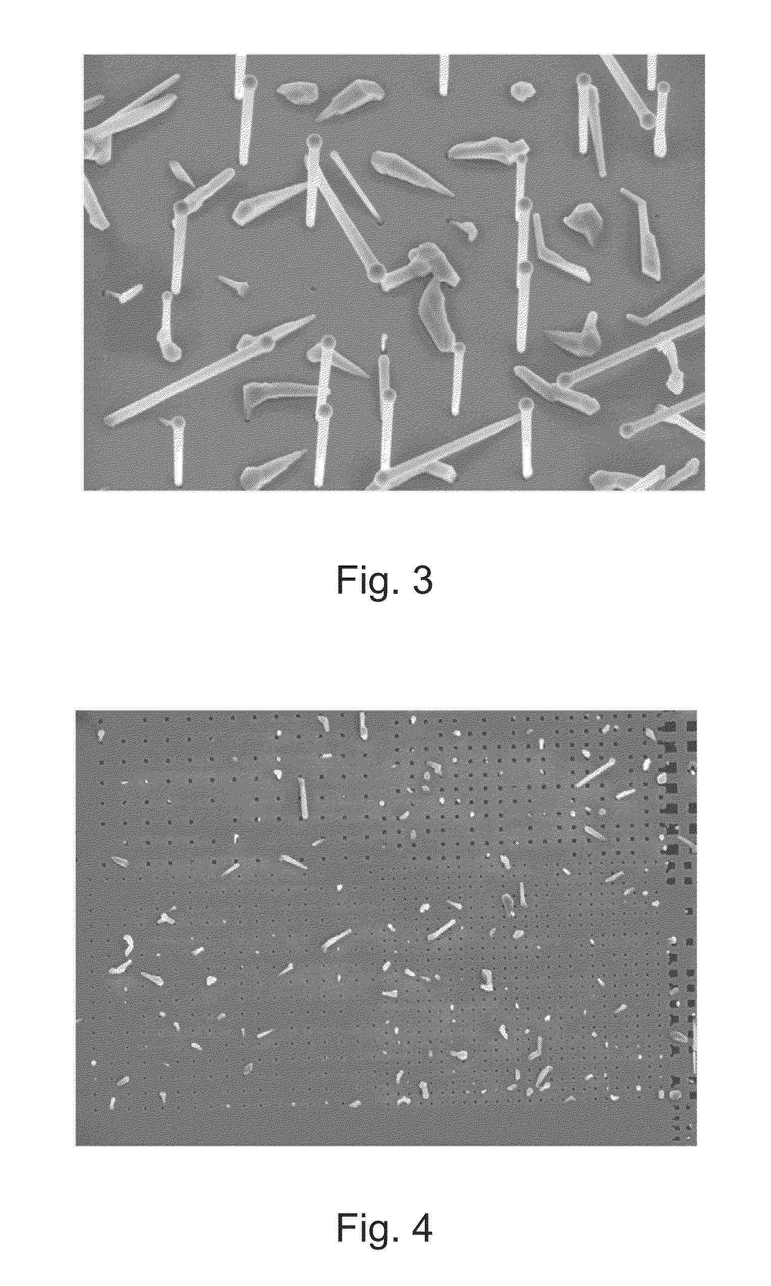
[0057]In example 1, growth of GaAsP nanowires on a patterned substrate was performed in an molecular beam epitaxy (MBE) apparatus in line with the stages set out in Table 2. Similarly to the comparative example above, the substrate was a quadrant of semiconductor wafer formed from p-type silicon., and the treatment surface was a (111) surface on which a layer of silicon dioxide having a array of holes fabricated therein was formed using the method described below with reference to FIG. 11. FIG. 5 shows a plan view of the substrate 200. FIGS. 6, 7 and 8 are SEM images taken at respective sub-regions 202, 204, 206 on the surface.

TABLE 2Growth parameters for example 1TimeTGa FluxV / IIIAs2 FluxP Flux(mins)(° C.)De-ox 1————5900De-ox 2————10880Warm-up——2.6 × 10−66.1 × 10−75Growth1.6 × 10−7202.6 × 10−66.1 × 10−740~6380.5 ml / sStop / cool0—0~0100

[0058]Example 1 thus differs from the comparative example due to the presence of a preliminary de-oxidation step in which the substrate is heated in th...

example 2

[0061]In example 2, growth of GaAsP core nanowires on a patterned substrate was performed in an molecular beam epitaxy (MBE) apparatus in line with the stages set out in Table 3. The process was set up in the same way as example 1.

TABLE 3Growth parameters for example 2TimeTGa FluxV / IIIAs4 FluxP Flux(mins)(° C.)De-ox————20832Ga deposit1.6 × 10−7———16000.5 ml / sGrowth 11.6 × 10−733.7 × 10−71.1 × 10−756000.5 ml / sGrowth 21.6 × 10−768.5 × 10−71.1 × 10−7106000.5 ml / s[in 30 s]Growth 31.6 × 10−7101.40 × 10−6 2.0 × 10−7106000.5 ml / s[in 30 s]Growth 41.6 × 10−7152.11 × 10−6 2.9 × 10−756000.5 ml / s[in 30 s][in 30 s]Growth 51.6 × 10−7202.82 × 10−6 3.8 × 10−7156000.5 ml / s[in 30 s][in 30 s]Stop / cool0—8.5 × 10−71.1 × 10−7100 [in 0 s] [in 0 s]

[0062]In this example, the preliminary de-oxidation process is a single stage, performed at a lower temperature but for a longer period than in example 1. FIG. 9 is an SEM image showing the results of this growth process. Again it may be seen that the nanowire gr...

example 3

[0063]In example 3, growth of core-shell nanowires on a patterned solar cell substrate was performed in an molecular beam epitaxy (MBE) apparatus in line with the stages set out in Table 4. The process was set up in the same way as example 1.

TABLE 4Growth parameters for example 3TimeTGa FluxIn FluxV / IIIAs4 FluxP Flux(mins)(° C.)DopingDe-ox—————20832—Ga deposit1.6 × 10−7————1600—0.5 ml / sGrowth 11.6 × 10⁻⁷—33.7 × 10−71.1 × 10−75600Be0.5 ml / s1.5 × 10−17Growth 21.6 × 10⁻⁷—68.5 × 10−71.1 × 10−710600Be0.5 ml / s[in 30 s]1.5 × 10⁻¹⁷Growth 31.6 × 10⁻⁷—101.40 × 10⁻⁶ 2.0 × 10−710600Be0.5 ml / s[in 30 s]1.5 × 10⁻¹⁷Growth 41.6 × 10⁻⁷—152.11 × 10⁻⁶ 2.9 × 10−75600Be0.5 ml / s[in 30 s][in 30 s]1.5 × 10⁻¹⁷Growth 51.6 × 10⁻⁷—202.82 × 10⁻⁶ 3.8 × 10−715600Be0.5 ml / s[in 30 s][in 30 s]1.5 × 10⁻¹⁷Pause 10——2.82 × 10⁻⁶ 3.8 × 10−710485—Pause 20——6.7 × 10−62.9 × 10−610485—Shell-p1.6 × 10−7—606.7 × 10−62.9 × 10−66485Be0.5 ml / s  5 × 10⁻¹⁶Shell-i1.6 × 10−7—606.7 × 10−62.9 × 10−620485—0.5 ml / sShell-n1.6 × 10−7—606.7 ...


PUM

PropertyMeasurementUnit
thicknessaaaaaaaaaa
diameteraaaaaaaaaa
thicknessaaaaaaaaaa

Abstract

The present invention provides a reproducible preliminary in-situ oxide removal step for patterned self-assisted III-V semiconductor nanowire growth. Here “in-situ” means located within the same treatment environment or apparatus as the nanowire growth process, e.g. with a molecular beam epitaxy (MBE) apparatus or the like. Providing an in-situ process may prevent the formation of a thin oxide layer during transfer of the substrate into the nanowire growth apparatus.

Description

FIELD OF THE INVENTION[0001]The invention relates to the growth of semiconductor nanostructures, and in particular to the fabrication of an array of one-dimensional semiconductor nanostructures, e.g. nanowires or the like, by epitaxial growth on a substrate.BACKGROUND TO THE INVENTION[0002]Epitaxial growth of Group III-V semiconductor nanowires, such as GaAs, GaAsP, InAs, InP, GaAsSb, InSb or InAsSb nanowires, is important in areas like sensors, LEDs and photovoltaics. Much research in this field focusses on optimizing the growth parameters used to produce the nanowire structures.[0003]One known optimization is to avoid the use of a catalyst such as gold during growth in order to avoid contamination of the resulting nanowire crystal lattice or substrate. The optimization may be achieved by using a growth method known as “self-assisted growth”, or “self-catalysed growth”, in which for instance a gallium droplet is used to grow a Ga-based nanostructure, e.g. a GaAsP nanowire or an ind...

Claims


Application Information

Patent Timeline
Patent Type & Authority Applications(United States)
IPC IPC(8): H01L21/02H01L29/06H01L21/306H01L29/20
CPCH01L21/02603H01L29/20H01L29/0676H01L21/02538H01L21/02694H01L21/02636H01L21/30604B82Y40/00H01L21/02057H01L21/02381H01L21/02433H01L21/02543H01L21/02546H01L21/02631H01L21/02639H01L21/0331H01L21/31144
Inventor AAGESEN, MARTINZHANG, YUNYANWU, JIANGLIU, HUIYUN
Owner GASP SOLAR APS
Why Eureka
Try Eureka