Light emitting device with improved internal out-coupling and method of providing the same

a technology of light-emitting devices and internal out-coupling, which is applied in the direction of organic semiconductor devices, sustainable manufacturing/processing, final product manufacturing, etc., can solve the problem of additional roughening steps, and achieve the effect of improving the out-coupling structure and

Inactive Publication Date: 2015-10-29
OLEDWORKS GMBH
View PDF1 Cites 2 Cited by
  • Summary
  • Abstract
  • Description
  • Claims
  • Application Information

AI Technical Summary

Benefits of technology

[0010]The proposed light emitting device can be manufactured by pre-treating the glass substrate to induce the local disturbances of layer growth on the flat surface of the glass substrate, depositing the high refractive index layer on the flat surface so that the columnar cone shaped growth of the high refractive index layer due to the local disturbances generates the bumps on the top surface of the deposited layer, and depositing the transparent electrode layer of the light emitting layer structure on the top surface of the high refractive index layer. The bumps are thus over-coated with the layers of the light emitting device and induce sufficient scattering by subsequent reflections. An advantage of this process is that no additional roughening step by e.g. grinding, sandblasting and then long-lasting structural etching of the substrate, e.g. low n glass (float glass), is needed before deposition.
[0012]According to a second aspect which can be combined with the above first aspect, the flat surface of the glass substrate may comprise local changes in the chemical surface composition of the glass substrate. These local changes may also act as seed points or areas for the columnar cone shaped growth of the optically thick high refractive index layer. In a more specific exemplary implementation of the second aspect, the chemical surface composition of the glass substrate may comprises a material with an element with a different oxidation state which modifies initial growth inhibition by locally higher sticking coefficient and thus stronger growth of the high refractive index layer.

Problems solved by technology

Such a solution may be obtained by a rough interface or structured surface 60 between the substrate parts with high refractive index n and low refractive index n. However, an additional roughening step is required, e.g., by grinding, sandblasting and after that rather time-consuming structural etching of the glass (float glass) with low refractive index n is needed.

Method used


Image

  • Light emitting device with improved internal out-coupling and method of providing the same
  • Light emitting device with improved internal out-coupling and method of providing the same
  • Light emitting device with improved internal out-coupling and method of providing the same

Examples


first embodiment

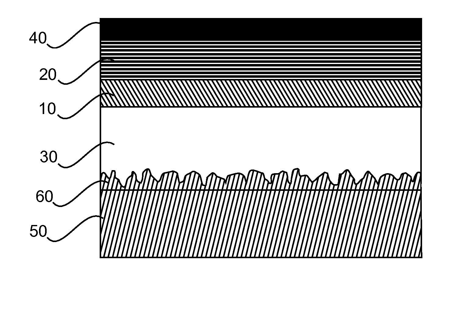
[0024]FIG. 2 shows a schematic cross sectional view of an OLED layer structure with improved columnar cone-shaped growth according to a The small ultrafine particles 12 or other surface defects on the surface 100 of the glass substrate induce locally different growth due to different sticking coefficients, with preferential columnar cone shaped growth, leading to bumps 14 of 0.5 to 4 μm, preferably 1 to 2 μm, cross-sectional dimension on the top surface of the CVD layer 11 underneath the lowest ITO layer (i.e. transparent electrode layer, e.g., anode layer 10) of the OLED layers 200 and the upper cathode layer 40. These bumps 14 are over-coated with the OLED layers 200 and induce sufficient scattering by subsequent reflections at several interfaces and at the cathode layer 40. The sticking coefficient is a term used in surface physics to describe the ratio of the number of adsorbate atoms (or molecules) that do adsorb, or “stick”, to a surface to the total number of atoms that impi...

second embodiment

[0027]In the following, a manufacturing process is described. An etching step is introduced as a pre-treatment of the glass substrate, which generates ultrafine particles deposited from the etching solution, which leads to local disturbancies of CVD layer growth. Thereby, relatively large lens like structures can be covered with much finer (mostly) bumps of only 0.5 to 4 μm, preferably 1 to 2 μm, extension. These bumps originated from growth disturbancies in the SiON CVD layer with high refractive index n. Hence, in consequence, it is no longer necessary to provide a rough surface base structure, but a flat glass substrates can be used with a suitable etching solution, eventually after etching a sacrificial glass plate, or by introducing ultrafine seed particles into the etching solution.

[0028]FIG. 4 shows a flow diagram of the manufacturing process according to the second embodiment. In step S401, the pre-treatment is done by exposure of the flat glass surface to a saturated etchi...

third embodiment

[0031]Thus, the pre-treatment of steps S401 and S402 of the above manufacturing process may be replaced by a step of providing local changes in the chemical surface composition of the glass substrate, e.g., by stronger oxidation (e.g. a material with an element with a higher or at least different oxidation state, thus modifying the initial growth inhibition by locally stronger growth).


PUM


Abstract

The present invention relates to a method of manufacturing a light emitting device with improved internal out-coupling by providing an intermediate layer (11) with a modulated surface. This is achieved by exposure of a flat glass surface (100) to a saturated etching fluid or by providing local changes in the chemical surface composition of the glass substrate or by depositing locally separated sub-μm particles. By removal of the etching fluid, either ultrafine particles (12) are deposited or defects are generated consisting of glass component areas of sub̂m-size extension with a high sticking coefficient with respect to the species deposited later on from the gas phase. These ultrafine particles or defects induce locally different growth by different sticking coefficients, with preferential columnar cone shaped growth, leading to small bumps (14) on the top surface of the intermediate layer (11), which are then over-coated with the layers (200) of the light emitting element and induce sufficient scattering by subsequent reflections.

Description

FIELD OF THE INVENTION[0001]The invention relates to the field of light emitting devices, more particular medium to large area (small molecule) organic light-emitting diodes, with layer structures comprising organic materials and being obtained by thermal evaporation in vacuum on a light transmitting substrate, e.g. float glass.BACKGROUND OF THE INVENTION[0002]In recent years, the technology of organic light-emitting diodes (OLEDs) has advanced considerably. The efficiency and lifetime of OLED devices have been improved dramatically and several kinds of OLED displays have been commercialized. OLEDs have many attractive features for display and general lighting applications. They have high brightness, high efficiency, a wide viewing angle, and quick response time. In addition, they can be fabricated by depositing or printing organic materials on a single substrate (e.g. glass substrate), and as such, make it possible to utilize the features of the substrate.[0003]An OLED is a light e...

Claims


Application Information

Patent Timeline
Patent Type & Authority Applications(United States)
IPC IPC(8): H01L51/52H01L51/00H01L51/56
CPCH01L51/5275H01L51/56H01L2251/308H01L51/5215H01L51/5209H01L51/0096H10K50/858Y02E10/549Y02P70/50H10K50/813H10K50/816H10K71/00H10K77/10H10K2102/103
Inventor GAERTNER, GEORG FRIEDRICHRIETJENS, GERARDUS HENRICUSBAKEN, JOANNA MARIA ELISABETH'T HART, JOHANNESLOEBL, HANS-PETER
Owner OLEDWORKS GMBH
Why Eureka
Try Eureka