

Shift Register and Display Device Using the Same
- Summary
- Abstract
- Description
- Claims
- Application Information
AI Technical Summary
Benefits of technology
Problems solved by technology
Method used
Image

Examples
first embodiment
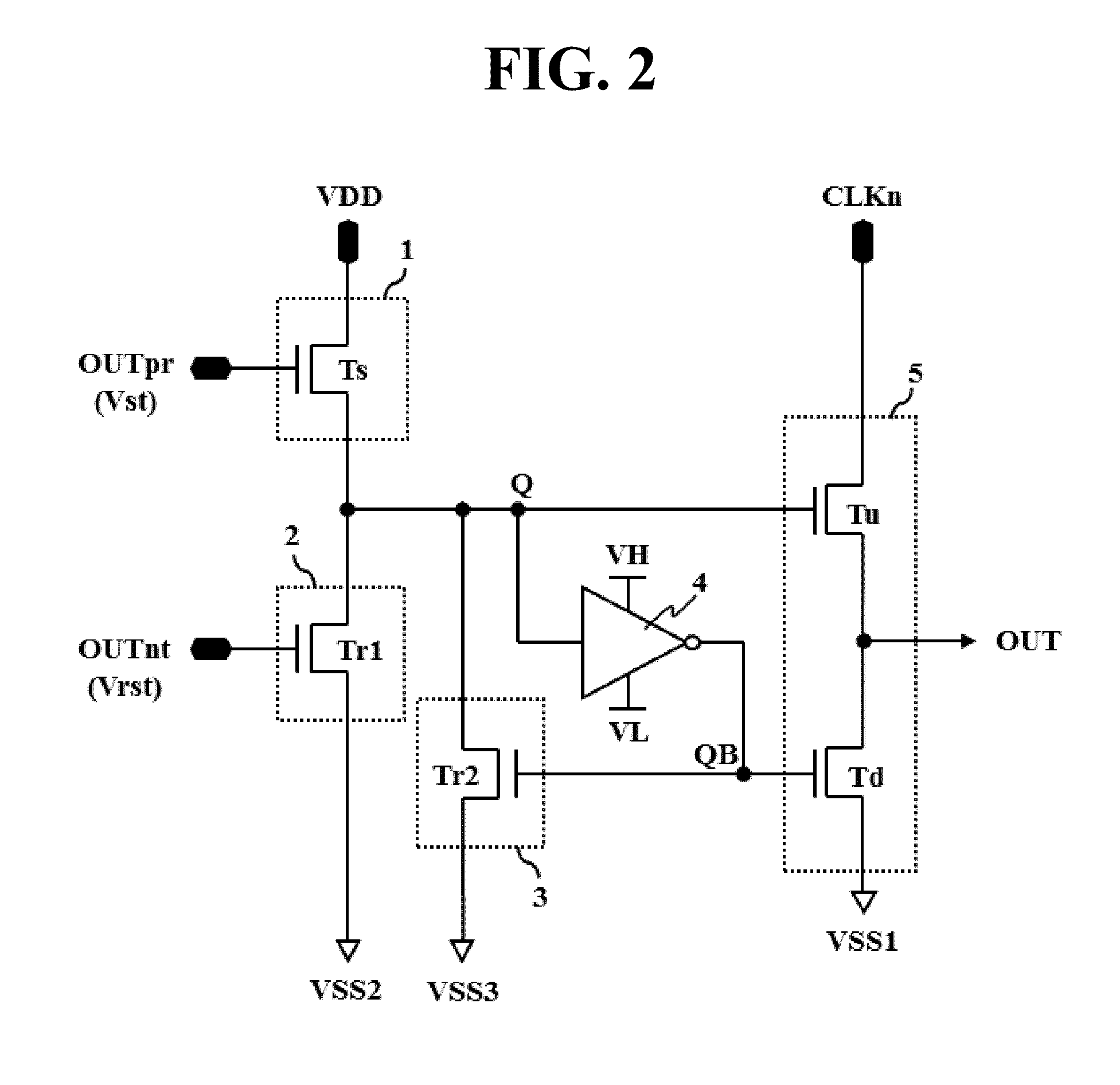
[0061]FIG. 2 is a circuit diagram showing the basic configuration of each stage in a shift register according to the present invention.
[0062]The stage shown in FIG. 2 includes a set unit 1, a reset unit 2, a noise cleaner 3, an inverter 4 and an output unit 5. The set unit 1, the reset unit 2 and the noise cleaner 3 may be referred to as a Q node controller for controlling a first control node (hereinafter, referred to as a Q node) and the inverter 4 may be referred to as a QB node controller for controlling a second control node (hereinafter, referred to as a QB node) of the output unit 5.
[0063]The set unit 1 sets the Q node to a high logic level in response to the scan output OUTpr from the previous stage. The set unit 1 includes a set transistor Ts for setting (charging) the Q node with a high voltage VDD as a set voltage in response to the high logic level of the previous scan output OUTpr. The set unit 1 of the first stage ST1 receives a start pulse Vst instead of the previous ...
second embodiment
[0081]FIG. 4 is a circuit diagram showing the basic configuration of each stage in a shift register according to the present invention.
[0082]The stage of the second embodiment shown in FIG. 4 is different from the stage of the first embodiment shown in FIG. 2 in that a noise cleaner 13 is composed of three transistors Ta, Tb and Tc. Thus, a description of the components equal to those of FIG. 2 will be omitted.
[0083]The noise cleaner 13 shown in FIG. 4 includes the first and second transistors Ta and Tb which are connected between the Q node and a third low voltage VSS3 terminal in series to reset the Q node with the third low voltage VSS3 in response to the logic state of the QB node and the third transistor Tc for supplying the high voltage VDD, that is, an offset voltage, to a connection node P of the first and second transistors Ta and Tb in response to the logic state of the Q node.
[0084]In order to prevent leakage current of the Q node via the reset unit 2 and the noise cleane...
third embodiment
[0088]FIG. 5 is a circuit diagram showing the basic configuration of each stage in a shift register according to the present invention.
[0089]The stage of the third embodiment shown in FIG. 5 is different from the stage of the first embodiment shown in FIG. 2 in that, as a carry output unit 6 for outputting a carry signal CR is further included, a carry signal CRpr from the previous stage is supplied to the set unit 1 and a carry signal CRnt from the next stage is supplied to the reset unit 2. Accordingly, a description of components equal to those of FIG. 2 will be omitted or given in brief.
[0090]A carry pull-up transistor Tcu of the carry output unit 6 outputs the input clock CLKn as the carry signal CR when the Q node is at a high logic level and a carry pull-down transistor Tcd outputs the third low voltage VSS3 (the second reset voltage) as the carry signal CR when the QB node is at a high logic level.
[0091]The set transistor Ts of the set unit 1 sets the Q node in response to t...
PUM
 Abstract
Description
Claims
Application Information