Semiconductor device

a technology of semiconductor devices and circuits, applied in semiconductor devices, semiconductor/solid-state device details, electrical apparatus, etc., can solve the problems of small space for wiring lines to be routed circuitously, affecting ca-system signals and i/o-system signals, and affecting signal asynchronously. , to achieve the effect of high-speed operation and small signal delay tim

Inactive Publication Date: 2015-11-05
PS4 LUXCO SARL
View PDF1 Cites 11 Cited by
  • Summary
  • Abstract
  • Description
  • Claims
  • Application Information

AI Technical Summary

Benefits of technology

[0011]Accordingly, the aim of the present invention is to resolve the abovementioned problems, and to provide a DDP-type semiconductor device in which CA-system wiring lines and I / O-system wiring lines do not readily become intertwined, and in which the lengths of the I / O-system conduction paths are made uniform, thereby making variability in the signal delay time small, and making high-speed operation possible.Means of Overcoming the Problems
[0014]The lengths of the conduction paths extending from the second electrodes and the fourth electrodes to the external electrodes are made uniform, and said conduction paths do not readily become intertwined with the conduction paths from the first electrodes and the third electrodes, and therefore in the semiconductor device there is little variability in the signal delay time (timing), and high-speed operation can be achieved.

Problems solved by technology

This gives rise to the problem that noise asynchronously affects CA-system signals and I / O-system signals.
The lengths of the wiring lines from the bond fingers on the reverse surface of the wiring board to the I / O external electrodes are therefore not uniform.
Further, because the region in which the wiring lines from the bond fingers to the I / O external electrodes and the region in which the CA external electrodes are disposed are close to one another, there is little space for the wiring lines to be routed circuitously, and the wiring lines cannot be routed circuitously.
In other words, the wiring lines from the bond fingers on the reverse surface of the wiring board to the I / O external electrodes are long, and the lengths of the conduction paths from the I / O-system electrode pads to the I / O external electrodes cannot be made uniform.
Thus the lengths of the conduction paths between the electrode pads on each semiconductor chip and the external electrodes are long and are not readily made uniform, and therefore the terminal capacitances of the external electrodes having long conduction paths are large, and ultimately variability in the signal delay time (timing) increases.

Method used


Image

  • Semiconductor device
  • Semiconductor device
  • Semiconductor device

Examples


embodiment

Second Mode of Embodiment

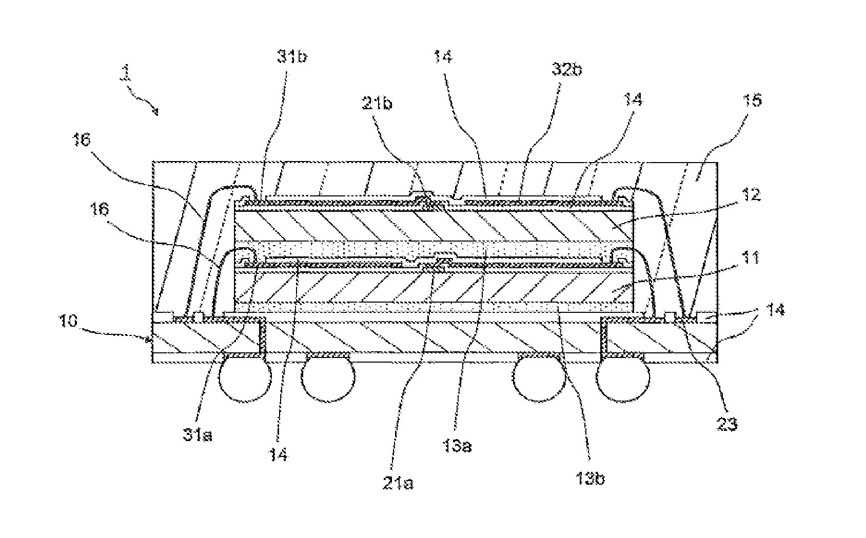
[0060]FIG. 5 is a cross-sectional view illustrating the configuration of a semiconductor device according to a second mode of embodiment of the present invention.

[0061]A DDP-type semiconductor device 1 comprises a first semiconductor chip 11 mounted on a wiring board 10, which has a substantially quadrilateral plate shape, and a second semiconductor chip 12 stacked on the first semiconductor chip 11. The configuration of the wiring board 10 is the same as in the first mode of embodiment and a description thereof is therefore omitted.

[0062]The first semiconductor chip 11 is mounted on the main surface of the wiring board 10 with the interposition of a bonding member (DAF) 13b.

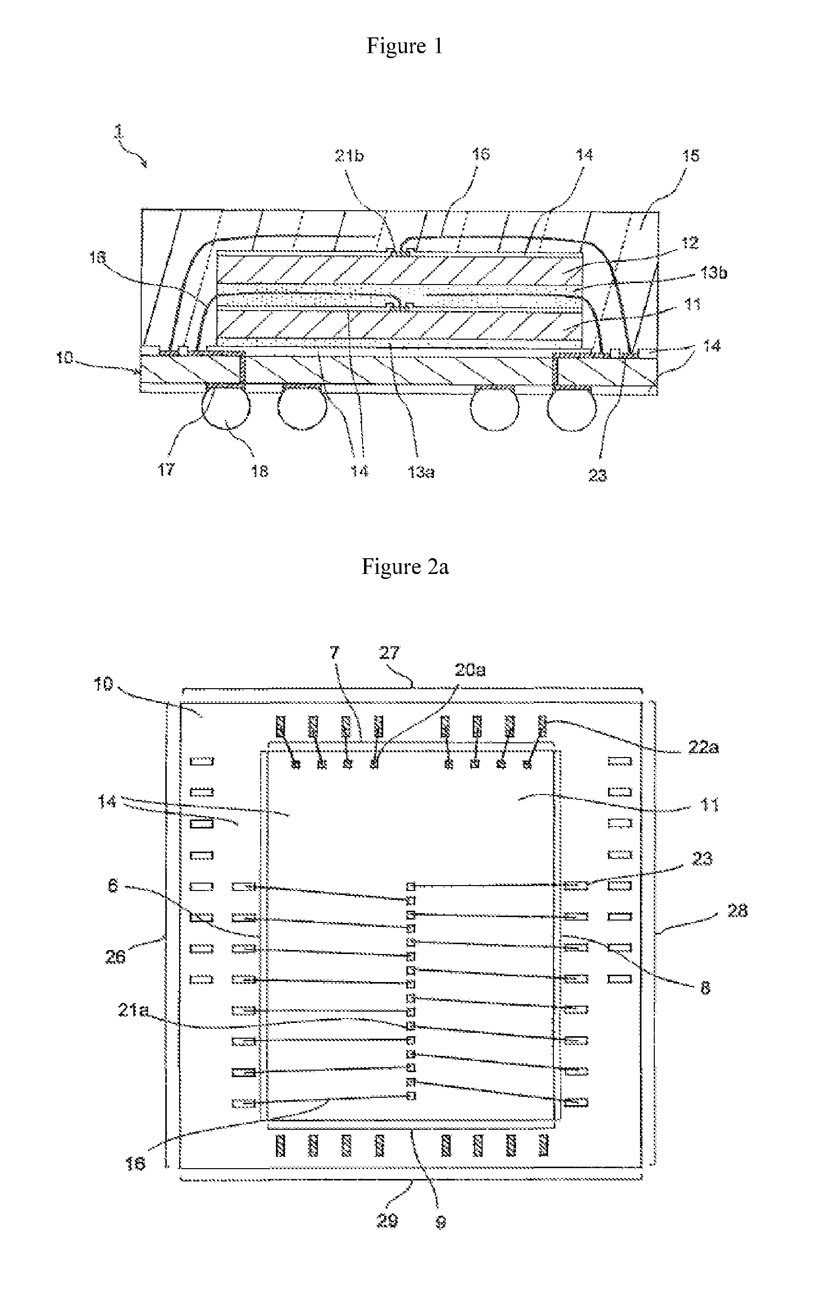
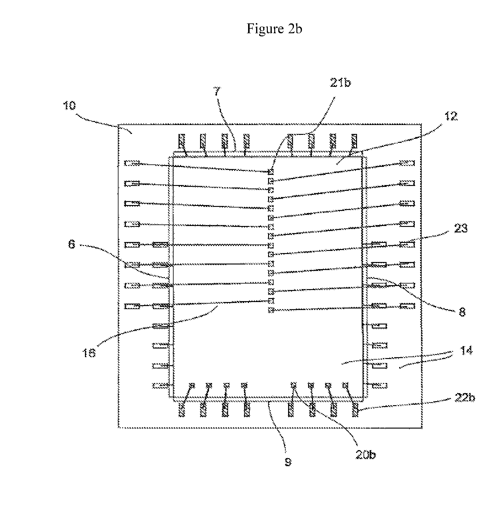
[0063]The first semiconductor chip 11 is in the shape of a substantially quadrilateral plate comprising first to fourth edges 6 to 9, and a memory circuit or the like (which is not shown in the drawings), and a plurality of electrode pads 20 and 21 are formed on its main surface. The fi...


PUM


Abstract

One semiconductor device has a wiring substrate, a first semiconductor chip, and a second semiconductor chip. Each semiconductor chip includes a first side and a third side which are opposed, a second side which is perpendicular to the first side, and a fourth side opposing the second side. A first electrode (CA electrode pad) parallel to the first side, and a second electrode (I / O electrode pad) arranged parallel to the second side near the second side, are provided on the first semiconductor chip. A third electrode (CA electrode pad) parallel to the first side, and a fourth electrode (I / O electrode pad) arranged parallel to the fourth side near the fourth side, are provided on the second semiconductor chip.

Description

TECHNICAL FIELD[0001]The present invention relates to a semiconductor device.BACKGROUND ART[0002]There has been an increased demand in recent years for the density of semiconductor devices mounted on circuit boards in compact electronic equipment such as mobile equipment to be increased to cope with reductions in the size of the equipment and increases in the level of functionality. To meet this demand, semiconductor devices in which a plurality of semiconductor chips are stacked on one wiring board have been devised. As one example thereof, patent literature article 1 (Japanese Patent Kokai 2011-249582) discloses a DDP (Dual Die Package) type semiconductor device in which two semiconductor chips are stacked on one wiring board.[0003]Semiconductor chips in which electrode pad rows comprising a plurality of electrode pads (electrodes) are formed on one surface (the main surface) are used as the semiconductor chips mounted in many DDP-type semiconductor devices. The plurality of elect...

Claims


Application Information

Patent Timeline
Patent Type & Authority Applications(United States)
IPC IPC(8): H01L25/065H01L23/00H01L23/498
CPCH01L25/0657H01L23/49838H01L2224/0235H01L2225/0651H01L2224/0237H01L24/02H01L24/97H01L2224/32145H01L2224/32225H01L2224/48091H01L2224/48227H01L2224/73265H01L2924/15311H01L2224/97H01L23/50H01L2924/181H01L2224/05554H01L2224/02379H01L2224/02375H01L2224/02381H01L2224/04042H01L2224/05548H01L2224/06135H01L2224/06136H01L2225/06565H01L2924/00014H01L2924/00H01L2924/00012H01L2224/83H01L2224/85
Inventor ISA, SATOSHI
Owner PS4 LUXCO SARL
Why Eureka
Try Eureka