Semiconductor optical integrated device

a technology of optical integrated devices and semiconductors, applied in the field of semiconductor optical integrated devices, can solve the problems of obstructing the monolithic integration of a wavelength-tunable laser, affecting the performance of the laser, and affecting the temperature requirements of the waveguide,

Inactive Publication Date: 2015-11-19
SUMITOMO ELECTRIC IND LTD
View PDF2 Cites 9 Cited by
  • Summary
  • Abstract
  • Description
  • Claims
  • Application Information

AI Technical Summary

Benefits of technology

[0007]Objects, features and advantages of the present invention will be understood more easily based on the following detailed description illustrating preferred embodiments of the invention with reference to the accompanying drawings.

Problems solved by technology

This difference becomes a barrier to monolithically integrating a wavelength-tunable laser and an optical modulator on a single substrate.
This difference in waveguide temperature requirements obstructs the monolithic integration of a wavelength-tunable laser and an optical modulator on a single substrate.

Method used


Image

  • Semiconductor optical integrated device
  • Semiconductor optical integrated device
  • Semiconductor optical integrated device

Examples


example

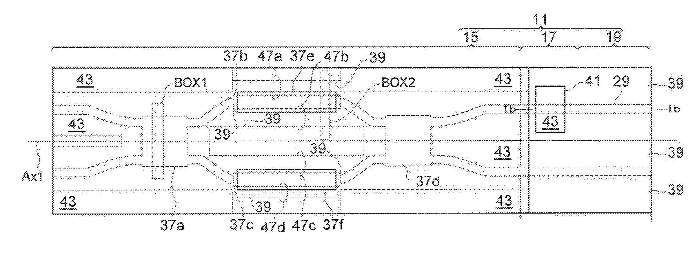
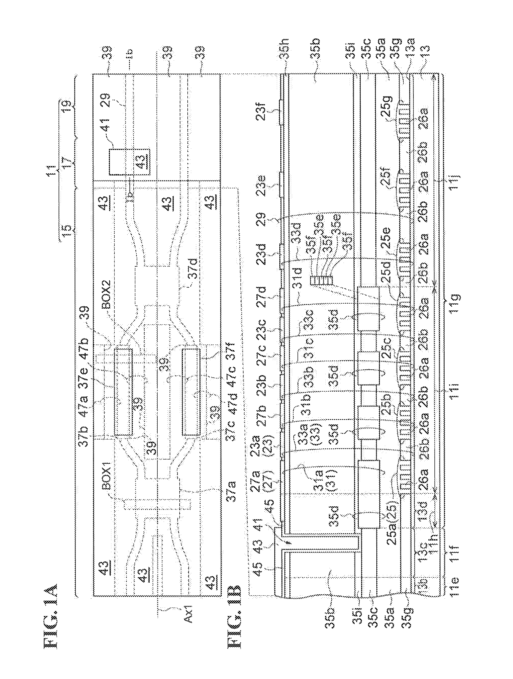
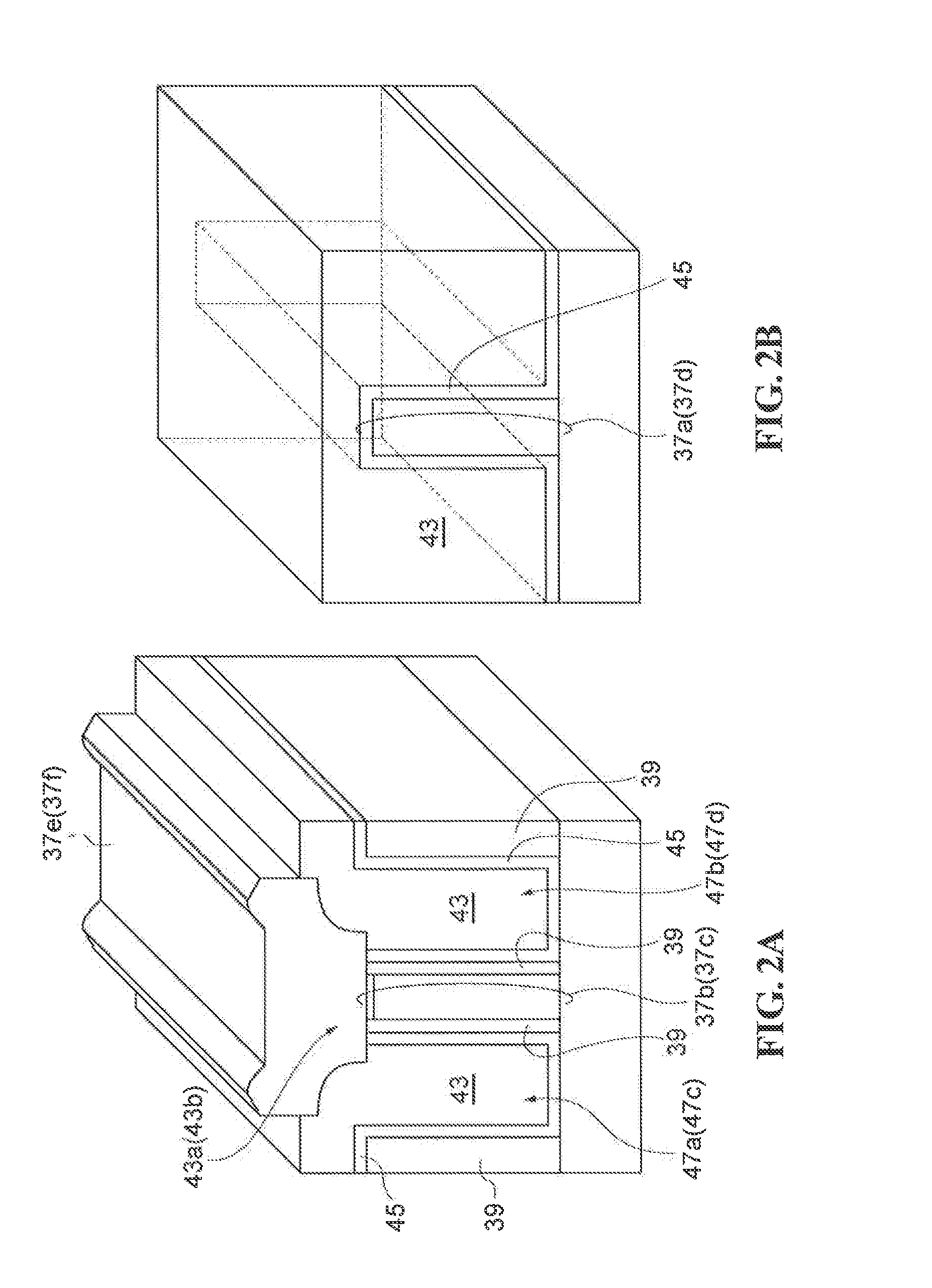
[0067]First, crystals are grown on an n-type InP substrate by an OMVPE method to form an n-type InP buffer layer and an n-type GaInAsp grating layer (bandgap wavelength: 1300 nm). Next, the n-type GaInAsP grating layer is treated by an interference exposure method or a nano-imprint method to form a pattern of gratings. The n-type GaInAsP grating layer is etched by dry etching using CH4 / H2 gas. This processing results in sampled gratings. After this formation, the patterned n-type GaInAsp grating layer is buried with InP by crystal growth using an OMVPE method. Subsequently, an n-type GaInAsP optical confinement layer (bandgap wavelength: 1200 nm), an undoped GaInAsP quantum well multilayer structure, an undoped optical confinement layer (bandgap wavelength: 1200 nm) and an undoped InP cap layer are grown. The quantum well multilayer structure has a bandgap wavelength of 1.55 μm and includes well layers and barrier layers. For example, the well layers include undoped GaInAsP having a...


PUM

PropertyMeasurementUnit
thicknessaaaaaaaaaa
refractive indexaaaaaaaaaa
thicknessaaaaaaaaaa

Abstract

A semiconductor optical integrated device including: a substrate having a first area, a second area and a third area arranged in a waveguiding direction; a laser portion disposed on the third area the laser portion including a laser waveguide and a heater thereon; a semiconductor waveguide disposed on the second area, the semiconductor waveguide including a core layer and a cladding layer disposed on the core layer; a Mach-Zehnder modulator portion disposed on the first area, the Mach-Zehnder modulator portion including a first arm and a second arm; a buried region embedding the laser waveguide, the semiconductor waveguide, and the first and second arms; a groove disposed on the second area, the groove extending in a direction intersecting the waveguiding direction to across the semiconductor waveguide to the buried region; and a resin body disposed on the Mach-Zehnder modulator portion. The laser portion is optically coupled to the Mach-Zehnder modulator portion via the semiconductor waveguide. The groove has a bottom on a surface of the core layer of the semiconductor waveguide.

Description

BACKGROUND OF THE INVENTION[0001]1. Field of the Invention[0002]The present invention relates to semiconductor optical integrated devices.[0003]2. Description of the Related Art[0004]Patent Literature 1 (Japanese Unexamined Patent Application Publication No. 2008-010484) discloses a semiconductor optical device in which a laser section and an optical modulator section are monolithically integrated. In the semiconductor optical device of Patent Literature 1, the optical modulator region has a ridge waveguide structure buried with an organic insulating material. The laser section has a ridge waveguide structure in which peripheral regions of the mesa are not buried in an organic insulating material or a semiconductor, namely, the side surfaces of the ridge waveguide structure are exposed to air, Patent Literature 2 (Japanese Unexamined Patent Application Publication No. 2013-033892) discloses a wavelength-tunable laser. In wavelength-tunable lasers, the refractive index of optical wav...

Claims


Application Information

Patent Timeline
Patent Type & Authority Applications(United States)
IPC IPC(8): G02F1/225
CPCG02F2001/212G02F1/2257G02F1/2255G02F1/212H01S5/0261H01S5/0265H01S5/06256H01S5/06258H01S5/1209H01S5/1212H01S5/1215H01S5/2275
Inventor YAGI, HIDEKI
Owner SUMITOMO ELECTRIC IND LTD
Why Eureka
Try Eureka