

Display panel and method for manufacturing the same, and display device
a technology of display panel and display device, which is applied in the direction of static indicating device, instruments, optics, etc., can solve the problem of not being convenient for users to charge the cell
- Summary
- Abstract
- Description
- Claims
- Application Information
AI Technical Summary
Benefits of technology
Problems solved by technology
Method used
Image

Examples
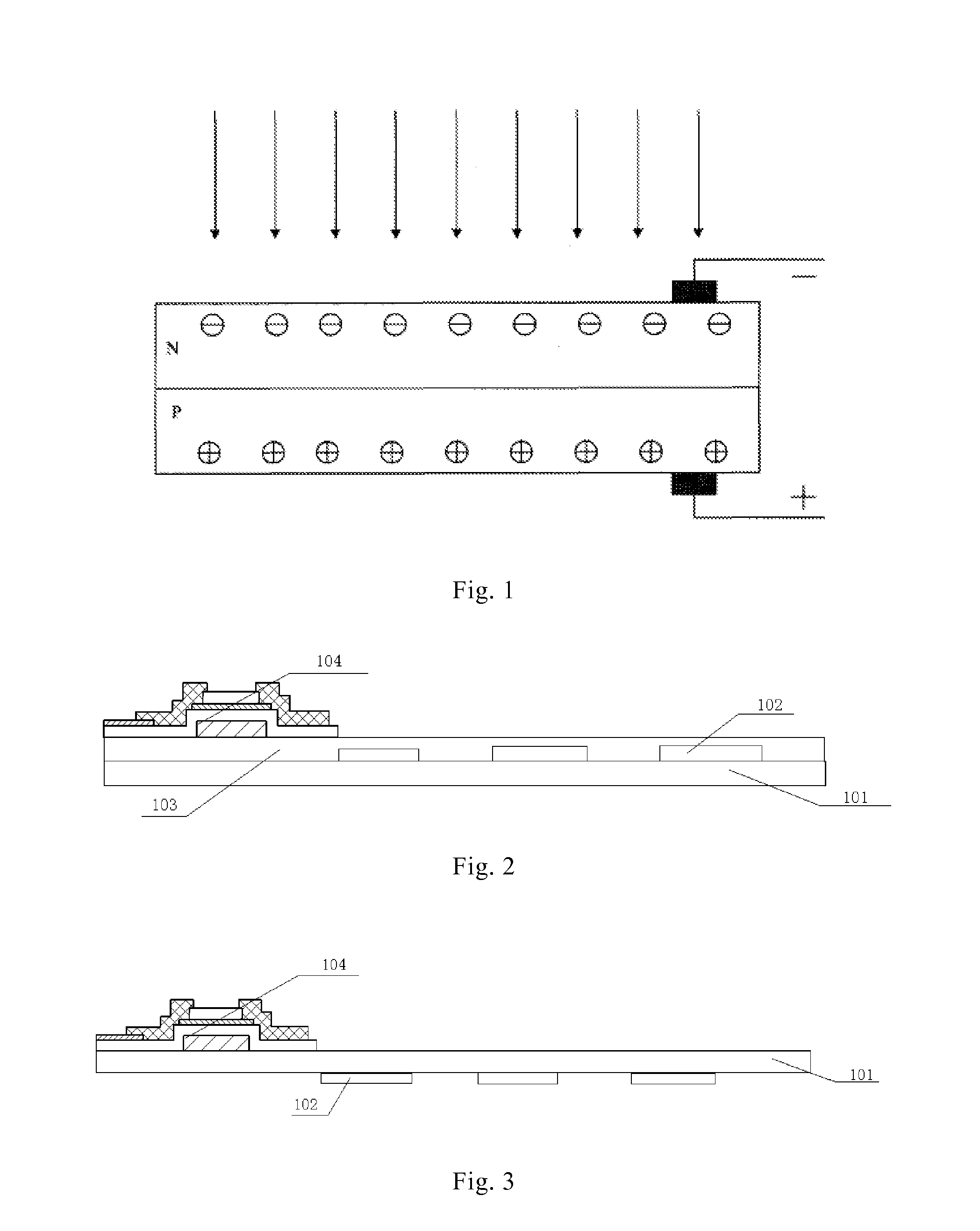
embodiment 1
[0047]The display panel of the embodiment includes an array substrate. As Embodiment 1, as shown in FIG. 2, the array substrate includes a first base substrate 101, an insulating layer 103 and a thin film transistor 104, and solar cells 102 are provided on the first base substrate 101, the insulating layer 103 is provided above the solar cells 102, and the thin film transistor 104 is provided above the insulating layer 103.
[0048]The above is a case that the solar cells 102 are provided at a light-transmissive region of the array substrate, and in this case, when the array substrate is irradiated by light, the solar cells 102 can absorb a certain amount of light to convert light energy into electric energy for storing, and then supply power to energy consumpting components of the display panel.
[0049]Of course, the solar cells 102 may be also provided on a prepared array substrate. That is to say, the array substrate may include the first base substrate 101, components such as the thi...
embodiment 2
[0050]The display panel of the embodiment includes an array substrate. As Embodiment 2, as shown in FIG. 3, the array substrate includes a first base substrate 101, wherein a thin film transistor 104 is provided on an upper surface of the first base substrate 101, and solar cells 102 are provided on a lower surface of the first base substrate 101.
[0051]The above is another case that the solar cells 102 are provided at a light-transmissive region of the array substrate, and in this case, when the array substrate is irradiated by light, the solar cells 102 can absorb a certain amount of light to convert light energy into electric energy for storing, and then supply power to energy consumpting components of the display panel.
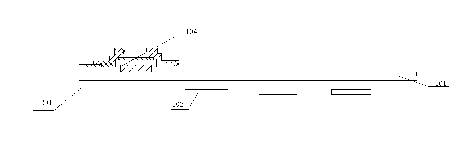
embodiment 3
[0052]The display panel of the embodiment includes an array substrate. As Embodiment 3, as shown in FIG. 4, the array substrate includes a first base substrate 101 and a second base substrate 201, a thin film transistor 104 is provided on an upper surface of the first base substrate 101, solar cells 102 are provided on a lower surface of the second base substrate 201, wherein a lower surface of the first base substrate 101 is attached to an upper surface of the second base substrate 201.
[0053]The above is yet another case that the solar cells 102 are provided at a light-transmissive region of the array substrate, and in this case, when the array substrate is irradiated by light, the solar cells 102 can absorb a certain amount of light to convert light energy into electric energy for storing, and then supply power to energy consumpting components of the display panel.
PUM
 Abstract
Description
Claims
Application Information