Method of Producing a III-V Fin Structure

Active Publication Date: 2015-11-26
INTERUNIVERSITAIR MICRO ELECTRONICS CENT (IMEC VZW) +1
View PDF6 Cites 5 Cited by
  • Summary
  • Abstract
  • Description
  • Claims
  • Application Information

AI Technical Summary

Benefits of technology

[0041]In embodiments of the present disclosure, this etch process is an anisotropic dry etch thereby further exposing the top surfaces of the at least two identical STI structures. Performing this anisotropic dry etch process may be advantageous as it allows directional etching of the diffusion barrier. Hence, the diffusion barrier is removed from the surface of the semiconductor substrate in between the STI structures as well as from the top surfaces of the STI structures. As a result, the diffusion barrier remains only on the sidewalls of the at least two identical STI structures. Performing this anisotropic etch process may be advantageous when providing the diffu

Problems solved by technology

Use of III-V substrates for the production of such FinFETs may be a challenging task due to III-V materials lacking thermally and electrically stable native oxides.
Such interface can lead to a high leakage path between gate, source, and/or drain regions of the transistor.
Although the problem of making FETs starting from a III-V substrate can be solved by the use of the passivation layer as disclosed in US 2011/0140229 A1, use of III-V material as the substrate material remains a challenge due to the production of FinFETs on III-V substrates being expensive.
Furthermore, it may be difficult to co-integrate of III-V channels and Ge channels, as Ge is a candidate for high-performance p-type FETs.
However, large lattice mismatch between III-V materials and silicon makes it a technological challenge to grow III-V materials on silicon.
Such large lattice mismatch between III-V materials and the Si substrate leads to the formation of crystalline defects, such as dislocations, anti-phase boundaries, twins a

Method used


Image

  • Method of Producing a III-V Fin Structure
  • Method of Producing a III-V Fin Structure
  • Method of Producing a III-V Fin Structure

Examples


Embodiment Construction

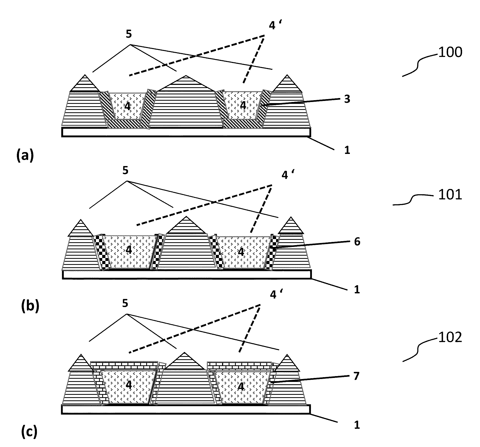
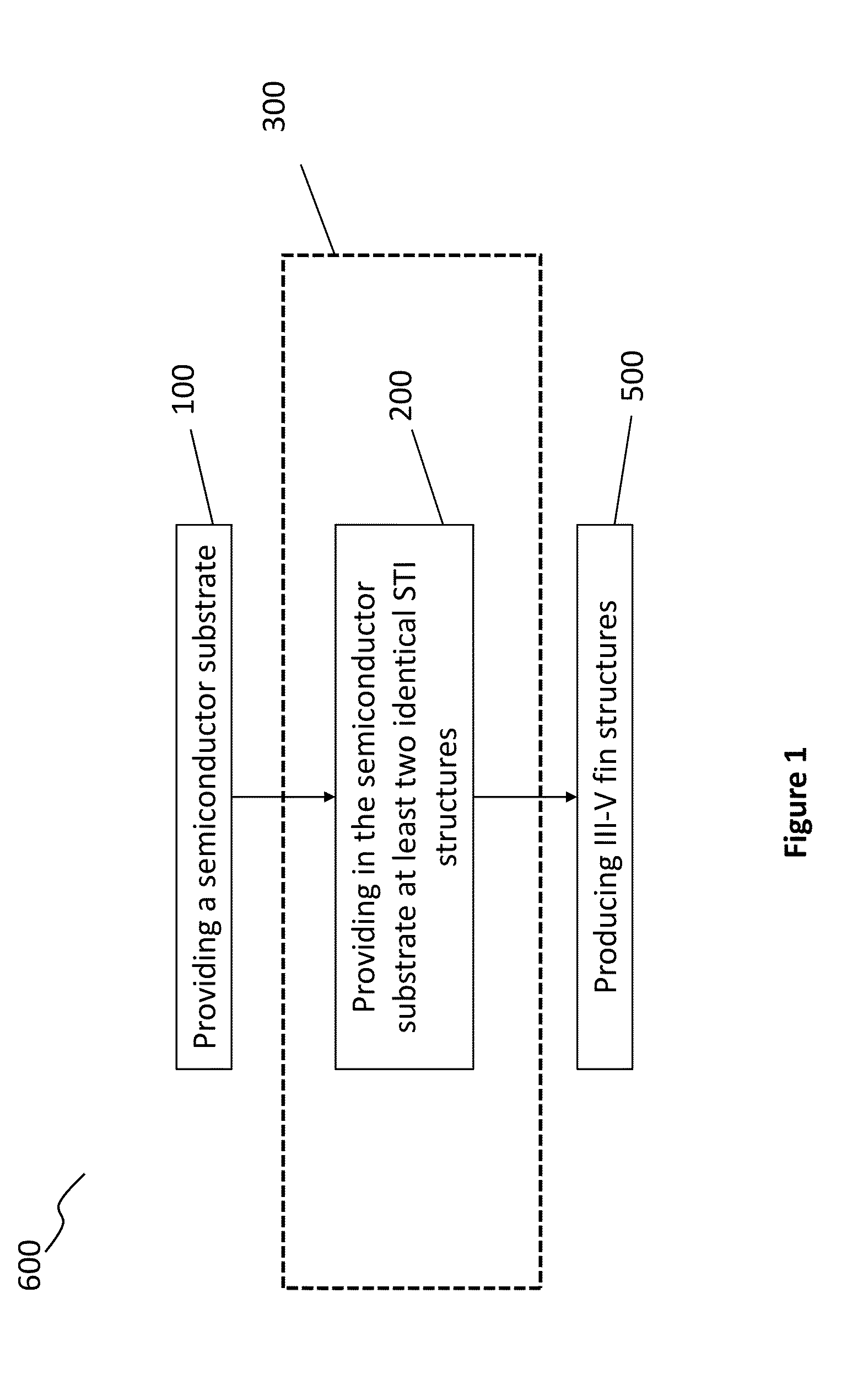
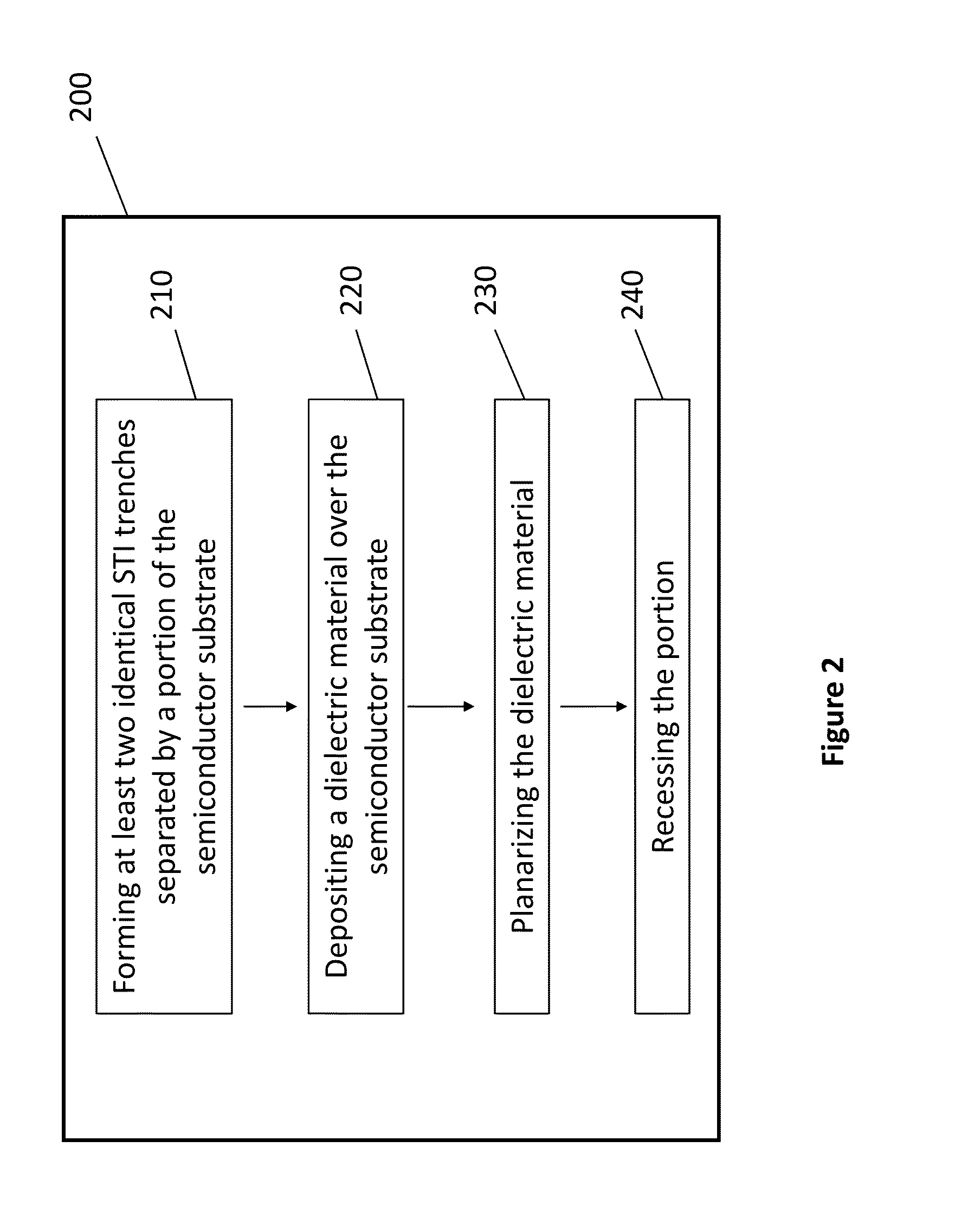
[0057]The present disclosure will be described with respect to particular embodiments and with reference to certain drawings but the disclosure is not limited thereto but only by the claims. The drawings described are only schematic and are non-limiting.

[0058]Reference throughout this specification to “one embodiment” or “an embodiment” means that a particular feature, structure or characteristic described in connection with the embodiment is included in at least one embodiment of the present disclosure. Thus, appearances of the phrases “in one embodiment” or “in an embodiment” in various places throughout this specification are not necessarily all referring to the same embodiment, but may. Furthermore, the particular features, structures or characteristics may be combined in any suitable manner, as would be apparent to one of ordinary skill in the art from this disclosure, in one or more embodiments.

[0059]Similarly, it should be appreciated that in the description of exemplary or e...


PUM


Abstract

A method of producing a III-V fin structure within a gap separating shallow trench isolation (STI) structures and exposing a semiconductor substrate is disclosed, the method comprising providing a semiconductor substrate, providing in the semiconductor substrate at least two identical STI structures separated by a gap exposing the semiconductor substrate, wherein said gap is bounded by said at least two identical STI structures, and, producing a III-V fin structure within said gap on the exposed semiconductor substrate, and providing a diffusion barrier at least in contact with each side wall of said at least two identical STI structures and with side walls of said III-V fin structure and wherein said semiconductor substrate is a Si substrate.

Description

CROSS-REFERENCE TO RELATED APPLICATION[0001]This application claims priority to European Patent Application No. 14169499.2 filed on May 22, 2014, the contents of which are hereby incorporated by reference.FIELD OF THE DISCLOSURE[0002]The present disclosure is related to the field of semiconductor processing. More specifically, it is related to a method of producing a III-V fin structure of a semiconductor device in a substrate.BACKGROUND OF THE DISCLOSURE[0003]CMOS scaling according to Moore's law has been providing the semiconductor industry with reduced transistor size while offering enhanced performance. However, in order to continue scaling, new channel materials having a high carrier velocity may be desirable.[0004]Field effect transistors (FinFETs) incorporating fin structures having III-V compound semiconductors as channel material are considered to be attractive candidates for high-performance n-type FETs in the semiconductor industry.[0005]Use of III-V substrates for the pr...

Claims


Application Information

Patent Timeline
IPC IPC(8): H01L29/78H01L29/06H01L29/66H01L21/3213H01L21/285H01L21/762H01L21/3205H01L29/20H01L21/02
CPCH01L29/7851H01L29/20H01L29/0653H01L29/66522H01L21/02538H01L21/0262H01L29/66795H01L21/2855H01L21/76224H01L21/32051H01L21/32053H01L21/32135H01L21/32134H01L21/28556H01L21/02543H01L21/02546H01L21/02579
Inventor MINARI, HIDEKIYOSHIDA, SHINICHIPOURTOIS, GEOFFREYCAYMAX, MATTYSIMOEN, EDDY
Owner INTERUNIVERSITAIR MICRO ELECTRONICS CENT (IMEC VZW)
Why Eureka
Try Eureka