Wafer processing method

a processing method and wafer technology, applied in the field of wafer processing method, can solve the problems of lowering the the quality of the device chip, and achieve the effect of lowering the quality

Active Publication Date: 2015-12-10
DISCO CORP
View PDF3 Cites 4 Cited by
  • Summary
  • Abstract
  • Description
  • Claims
  • Application Information

AI Technical Summary

Benefits of technology

[0010]However, when the protective tape is adhered to the front side of the wafer formed continuously with the modified layers along the division lines and, in the condition where the protective tape side of the wafer is held onto a chuck table, the back side of the wafer is ground while supplying the grinding water to thin the wa

Problems solved by technology

However, when the protective tape is adhered to the front side of the wafer formed continuously with the modified layers along the division lines and, in the condition where the protective tape side of the wafer is held onto a chuck table, the back side of the wafer is ground while supplying the grinding water to thin the wafer to a predetermined thickness and divide the wafer into the individual device chips, there arises a problem that the grinding water penetrates through the gaps between the individually split device chips to contaminate the side surfaces and the front surfa

Method used


Image

  • Wafer processing method
  • Wafer processing method
  • Wafer processing method

Examples


Embodiment Construction

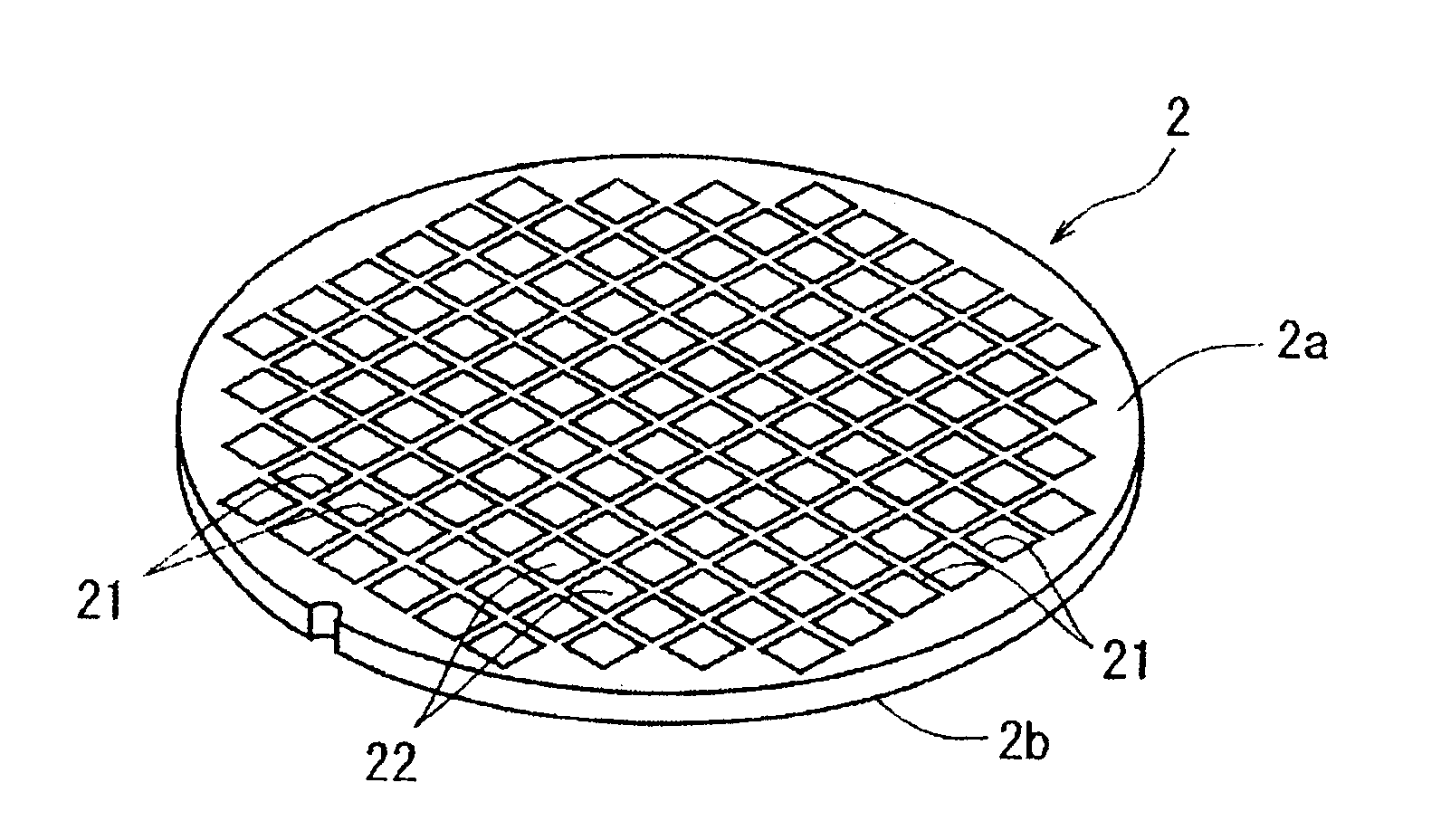
[0028]Some preferred embodiments of a wafer processing method and a dividing apparatus according to the present invention will be described in detail below, referring to the attached drawings. FIG. 1 shows a perspective view of a semiconductor wafer 2 to be processed according to the present invention. The semiconductor wafer 2 depicted in FIG. 1 is composed of a silicon wafer having a thickness of, for example, 500 μm. On a front side 2a of the semiconductor wafer 2, a plurality of division lines 21 are formed in a grid pattern, and a device 22 such as an IC and an LSI is formed in each of a plurality of regions partitioned by the division lines 21. A description will now be made of a wafer processing method for dividing the semiconductor wafer (hereinafter also referred to simply as “wafer” for short) 2 along the division lines 21 into the individual devices (device chips) 22.

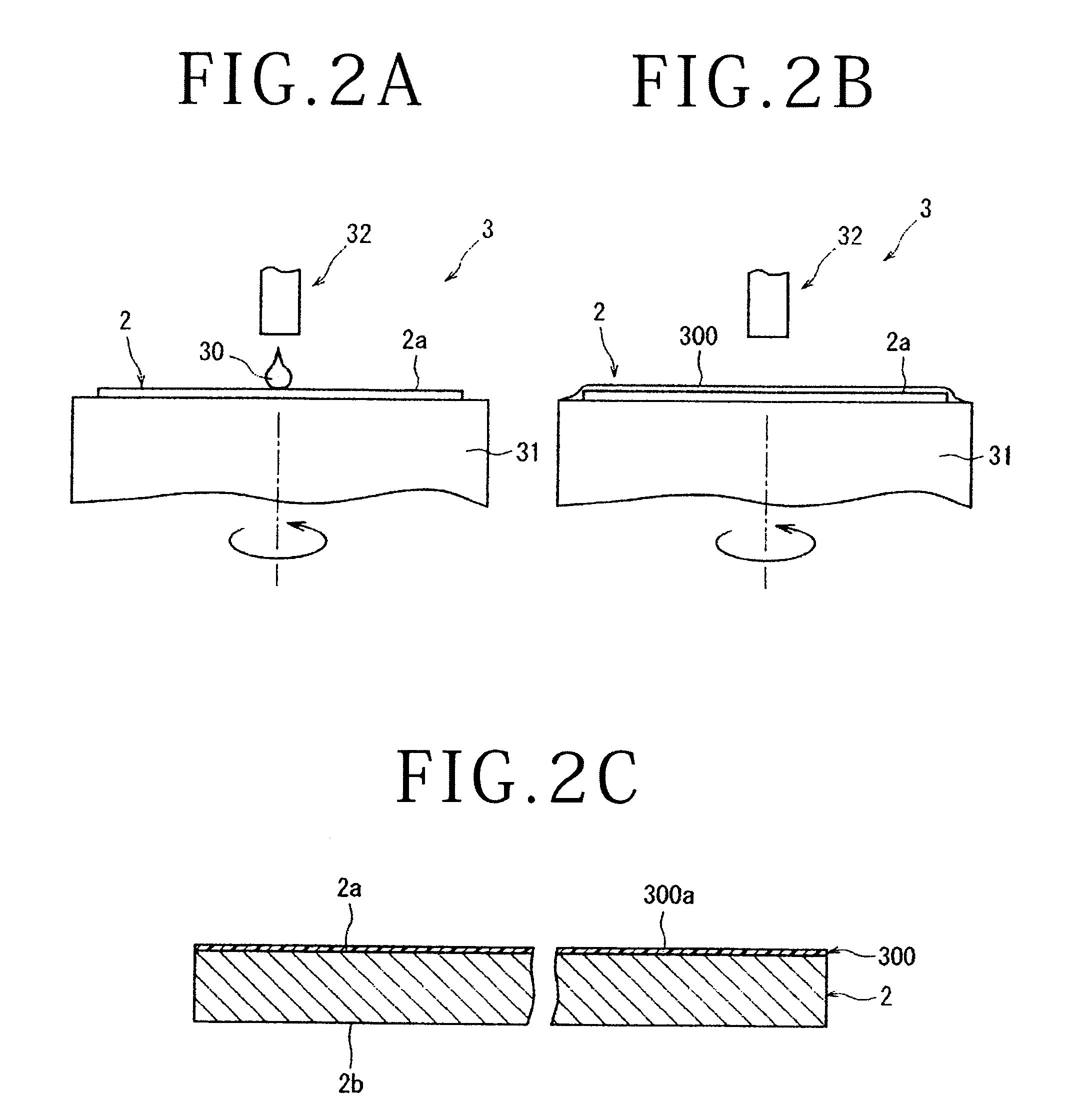
[0029]First, a protective film forming step is performed in which a liquid resin is applied to the front s...


PUM


Abstract

In a wafer processing method, a protective film is formed by applying a liquid resin to the front side of a wafer. A protective tape is adhered to a surface of the protective film. A modified layer is formed by applying a laser beam having such a wavelength as to be transmitted through the wafer along each of division lines, with a focal point positioned inside the wafer. The modified layer is formed inside the wafer along each of the division lines. The back side of the wafer is ground while supplying grinding water to thin the wafer to a predetermined thickness and to crack the wafer along the division lines using the modified layers as crack starting points so as to divide the wafer into individual device chips, after the protective film is formed, the protective tape is adhered, and the modified layer is formed.

Description

BACKGROUND OF THE INVENTION[0001]1. Field of the Invention[0002]The present invention relates to a wafer processing method by which a wafer having a plurality of division lines formed in a grid pattern on a front side thereof and having devices formed in a plurality of regions partitioned by the division lines is divided along the division lines.[0003]2. Description of the Related Art[0004]In a semiconductor device manufacturing process, a plurality of regions are partitioned by division lines arranged in a grid pattern on the front side of a semiconductor wafer having a substantially circular disk-like shape, and devices such as ICs and LSIs are formed in the thus partitioned regions. The thus formed semiconductor wafer is cut up along the division lines to divide the regions in which the devices are formed, thereby producing the individual device chips.[0005]The cutting of the semiconductor wafer along the division lines as above is ordinarily conducted by use of a cutting apparat...

Claims


Application Information

Patent Timeline
IPC IPC(8): H01L21/683H01L21/02H01L21/82
CPCH01L21/6836H01L21/02076H01L21/82H01L21/304H01L21/67092H01L21/67132H01L21/78H01L2221/68327H01L2221/6834
Inventor NAKAMURA, MASARU
Owner DISCO CORP
Why Eureka
Try Eureka