

Silicon carbide semiconductor device and method for manufacturing same
- Summary
- Abstract
- Description
- Claims
- Application Information
AI Technical Summary
Benefits of technology
Problems solved by technology
Method used
Image

Examples
examples
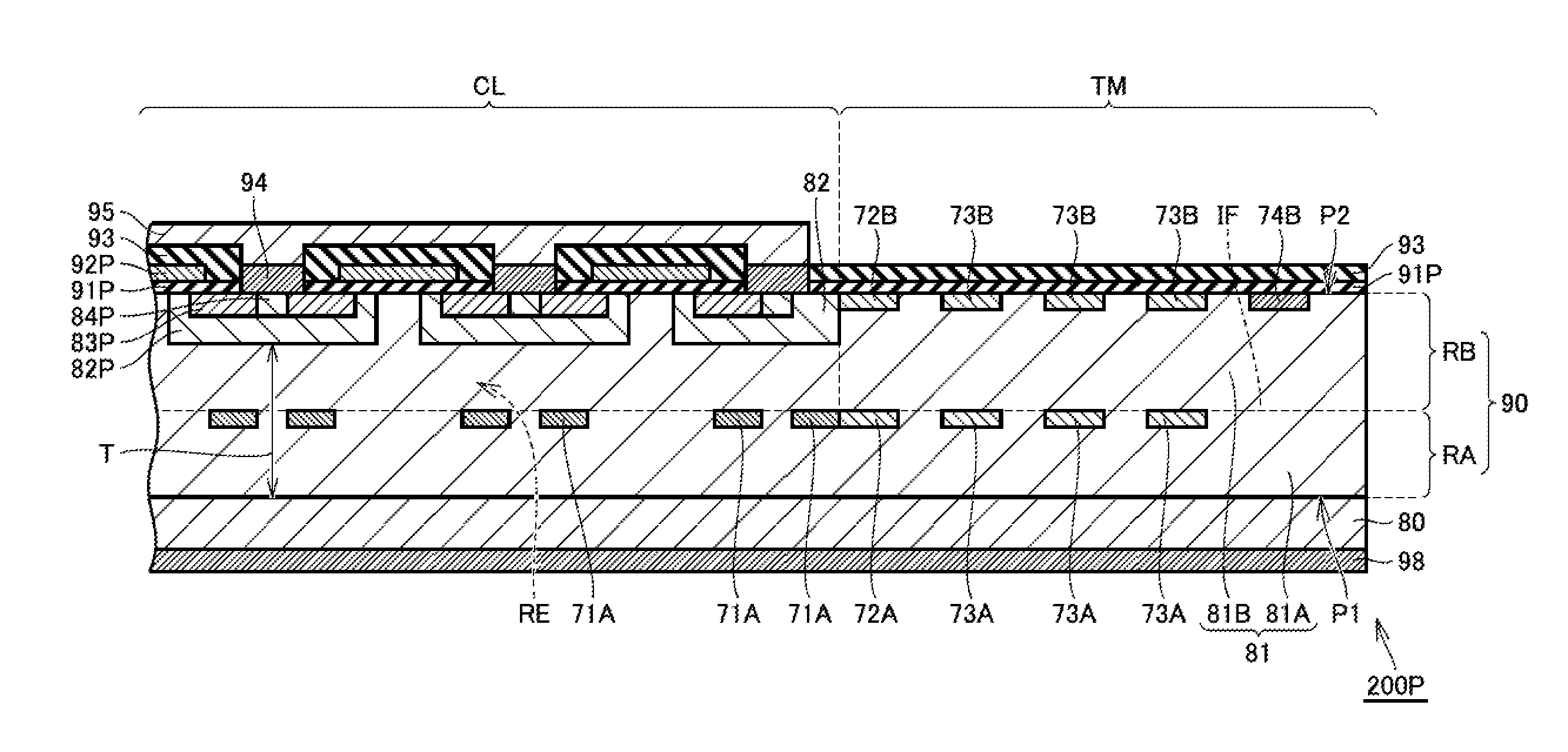
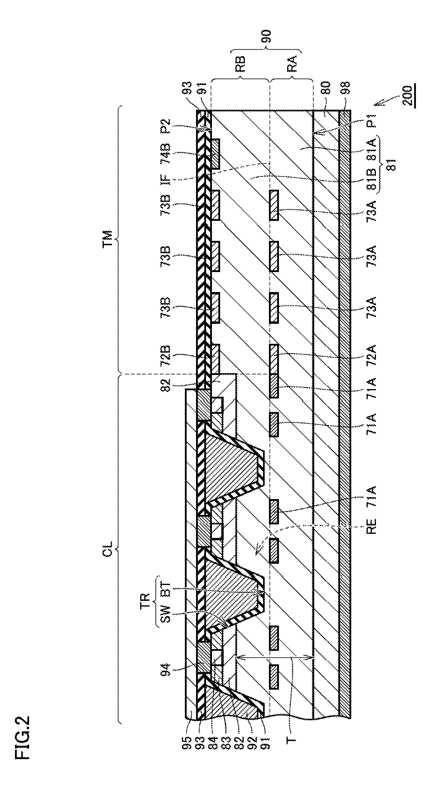
[0113]Table 1 below shows results of simulation for Examples 1 and 2 and a Comparative Example with regard to MOSFET 200 (FIG. 2).
TABLE 1ComparativeExampleExample 1Example 2Impurity Dose1 × 1013 (cm−2)3 × 10¹³ (cm−2)5 × 10¹³ (cm−2)AmountVoltage with which656 (V)1288 (V)1543 (V)Gate Oxide Film isBrokenVoltage with which2500 (V) 1540 (V)1450 (V)ChargeCompensationRegion is BrokenBreakdown Voltage656 (V)1288 (V)1450 (V)
[0114]In Table 1, the “Impurity Dose Amount” represents the impurity dose amount of charge compensation region 71A From this result, it is found that by increasing the impurity dose amount, the determination factor for breakdown voltage is changed from the breakage phenomenon of gate oxide film 91 to the breakage phenomenon of the charge compensation region. Moreover, it is found that the breakdown voltage of MOSFET 200 can be increased
[0115]With reference to FIG. 23, gate oxide film 91 is prevented from being broken as described above because electric field strength Box ...
PUM
 Abstract
Description
Claims
Application Information