Nanophotonic spatial light modulator

a spatial light modulator and photonic technology, applied in the field of nanophotonic devices, can solve the problems of limiting the switching speed of slms equipped with liquid crystals to a frequency range far below current telecommunication data manipulation rates, and current slms based on liquid crystal elements are only capable of covering a limited wavelength range, so as to achieve high pixel density, wide range of effects

Active Publication Date: 2015-12-31
OXFORD UNIV INNOVATION LTD
View PDF0 Cites 22 Cited by
  • Summary
  • Abstract
  • Description
  • Claims
  • Application Information

AI Technical Summary

Benefits of technology

[0048]Accordingly, the nanophotonic matrix array may combine a matrix of dielectric waveguides with individual nanoscale elements comprising the suitable phase-change material, wherein each individual nanoscale element may be optically addressed as an individual pixel within the nanophotonic matrix array, thus, allowing implementing arbitrary refractive index profiles which may be switched on a picosecond time scale owing to the ultra-fast phase transition of the phase-change material GST.
[0049]In a further aspect, the present invention relates to a use of the nanophotonic matrix array as described above and / or below as a spatial light modulator (SLM), preferably for shaping and / or steering a light beam, in all areas of optics, such as astronomy, microscopy, or lithography. This use is possible due to the matrix of PCM-based spatially addressable refractive index pixels as described above and / or below which is ideally suited to serve as an ultra-fast SLM which may be operated on a nanosecond and / or picosecond time scale. Since the operation principle as described herein comprises a more general approach, further applications may refer to ultra-fast optical filters as well as to applications in beam steering and beam shaping. In addition, since the absorption properties of the phase-change material, such as GST, may be strongly altered, the nanophotonic matrix may also be employed as a tunable optical mirror and / or a tunable optical absorber. Further applications may concern tunable grating structures and / or tunable matrix arrays being capable of operating in the Gigahertz range. Furthermore, a scalability of the nanophotonic device according to the present invention may enable a optical filter shaping on a single chip as well as a combination of a multitude or a plurality of such devices in order to form an integrated system. Consequently, multi-pixel imaging may be possible by manufacturing a large number of nanophotonic devices on the same chip, thus, providing a full two-dimensional image acquisition, preferably at single photon level, on a number of wavelength channels simultaneously.
[0050]In addition to the advantageous features as described above, the present invention may ideally be suited for an implementation of a widely tunable optical filter which may be spatially controlled. Using broadband transparent optical materials, such as saphir or glass as the substrate, may provide a large flexibility with regard to the operation wavelength of the nanophotonic matrix array in particular to be used as SLM. Within this respect, the respective device may be adaptable to the desired wavelength by scaling the size of the individual pixels which comprise the individual nanoscale elements from the visible to the infrared wavelength range. In addition, the wavelength range may further be extended by combining optical materials with transparency in the ultraviolet or the further infrared spectral range. Thus, the device according to the present invention may enable an operational bandwidth far above currently available devices and may, therefore, cover wavelengths which are hardly accessible with current SLMs.
[0051]Summarizing, the technology platform according to the present invention being related to nanophotonics and phase-change materials may particularly enable a manufacturing of integrated high-performance all-optically tunable photonic circuits. Using PCM nanoscale elements as switchable pixels may benefit from standard nanofabrication routines which are generally considered as fault-tolerant and as enabling fabrication of large-area matrix arrays. Consequently, the nanophotonic device as well as the nanophotonic matrix array according to the present invention may be fully scalable and suitable to implement optical devices, in particular SLMs, with a high pixel density over a large area. As a result, waver-scale fabrication procedures may also be employed here in order to implement functional miniaturized circuits having a potential for a reasonable prized mass production.

Problems solved by technology

As a result, optical elements which comprise liquid crystals are inherently slow owing to the limited switching speed of liquid crystals which usually lies in a low kilohertz range, thus, limiting the switching speed of SLMs being equipped with liquid crystals to a frequency range which is far below current telecommunication data manipulation rates.
In addition, current SLMs based on liquid crystal elements are only capable of covering a limited wavelength range.

Method used


Image

  • Nanophotonic spatial light modulator
  • Nanophotonic spatial light modulator
  • Nanophotonic spatial light modulator

Examples


Embodiment Construction

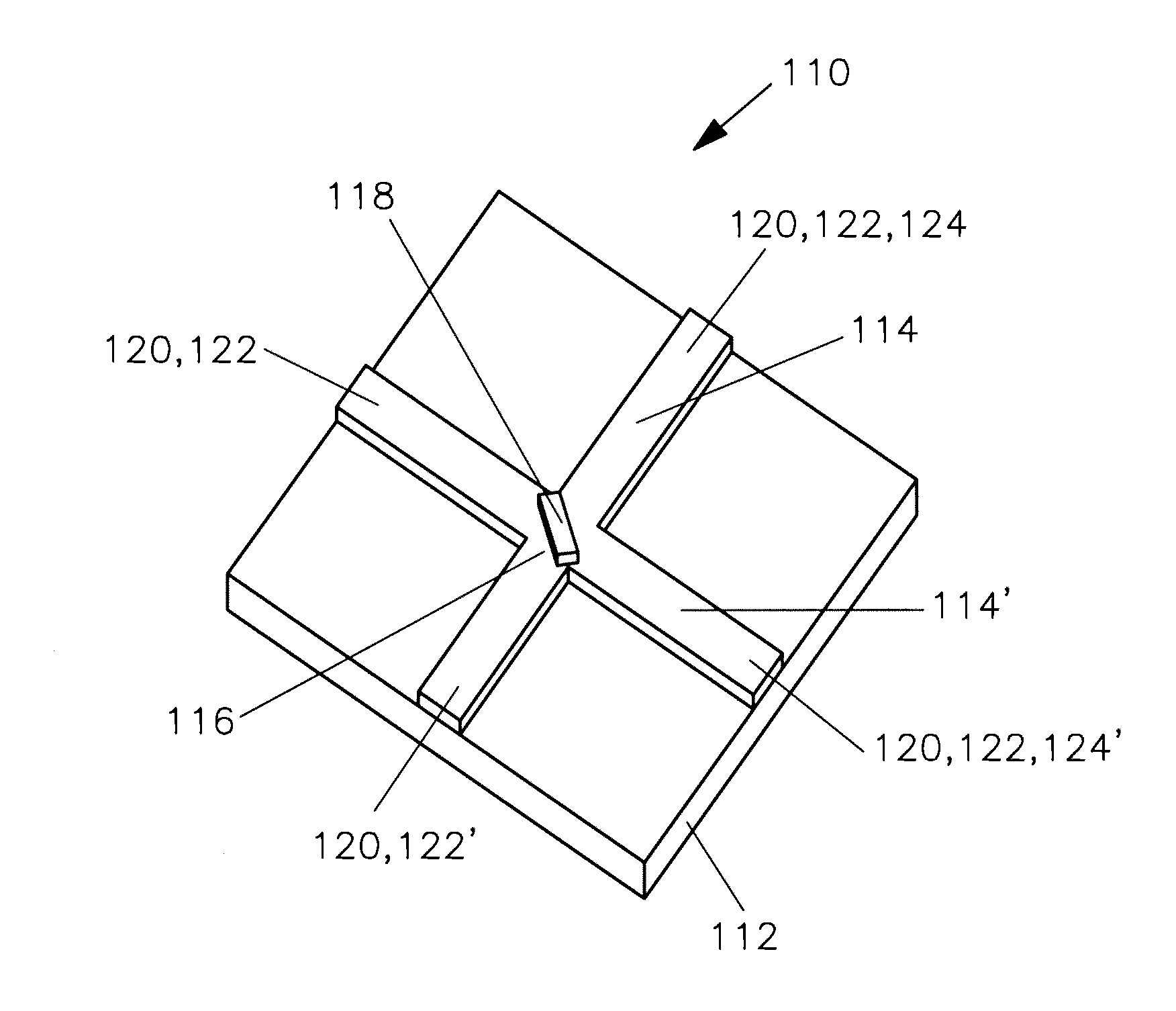
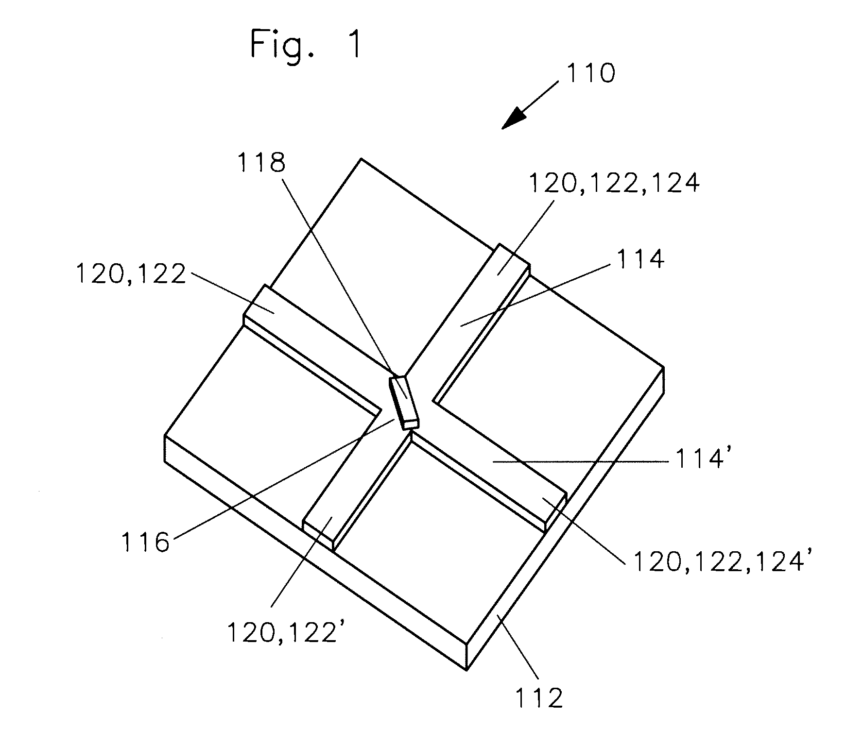
[0058]FIG. 1 schematically shows an aerial view of a preferred embodiment of a nanophotonic device 110 according to the present invention. On a transparent substrate 112, two waveguides 114, 114′ are located in a manner that they comprise a common intersection point 116. In this particular embodiment, the two waveguides 114, 114′ are arranged orthogonally with respect to each other, however, other arrangements are feasible where the two waveguides 114, 114′ adopt an angle≠90° with respect to each other.

[0059]According to the present invention, the nanophotonic device 110 further comprises a nanoscale element 118 at the intersection point 116. The nanoscale element 118 is switchable between two different states, wherein the two states differ by a refractive index value. In the examplary nanophotonic device 110 as presented in FIG. 1, this feature is obtained by selecting the nanoscale element 118 to comprise the chalcogenide-based phase-change material (PCM) Ge2Sb2Te5, usually abbrev...


PUM

PropertyMeasurementUnit
thicknessaaaaaaaaaa
thicknessaaaaaaaaaa
wavelengthsaaaaaaaaaa

Abstract

A nanophotonic device includes at least two waveguides located on top of a transparent substrate, which form an intersection point at which a part of a first waveguide simultaneously constitutes a part of a second waveguide. A nanoscale element located on top of the intersection point so that it partially or completely covers the intersection point is switchable between two different states, which differ by a refractive index value. The nanophotonic device is operated by injecting at least two optical pulses into the waveguides. Intensity of the optical pulses is selected so that a superposition of the optical pulses switches the nanoscale element into a desired state. Also disclosed is a nanophotonic matrix array in which parallel waveguides form nanophotonic devices. The nanophotonic matrix array may be used as a spatial light modulator (SLM), as an optical mirror, as an optical absorber, or as a tunable optical grating array.

Description

CROSS-REFERENCE TO RELATED APPLICATION[0001]This application claims priority from European Patent Application No. 14172938.4, filed Jun. 18, 2014. The contents of this application is incorporated herein by reference in its entirety.FIELD OF THE INVENTION[0002]The present invention is related to a nanophotonic device, to methods for its manufacturing and operating as well as to a nanophotonic matrix array and its use, in particular as a nanophotonic spatial light modulator (SLM).RELATED ART[0003]The present invention is located in the fields of nanophotonics and integrated optics as well as in the field of thin film technology with phase-change materials. A combination of these formerly separate fields of technology is intended to provide a new technology platform in order to implement integrated circuits, in particular nanophotonic integrated circuits, comprising additional degrees of freedom when compared to traditional photonic integrated circuits.[0004]Currently, phase-change mat...

Claims


Application Information

Patent Timeline
Patent Type & Authority Applications(United States)
IPC IPC(8): G02F1/01
CPCG02F1/365G02F1/19G02F1/3555G02B6/2804G02B6/2848G02B6/3556G02B6/3524G02B6/3546G02F1/3521G02B6/3596G02B6/3542G02F1/3137G02F1/3515G02F1/011G02F1/0126G02B6/00G02B6/107G02B6/12033G02B6/125G02B2006/12147
Inventor PERNICE, WOLFRAMBHASKARAN, HARISH
Owner OXFORD UNIV INNOVATION LTD
Why Eureka
Try Eureka