

Method for producing semiconductor device and semiconductor device
a semiconductor and device technology, applied in the direction of semiconductor devices, basic electric elements, electrical appliances, etc., can solve the problems of difficult to suppress leakage current, difficult to form deep contact holes, difficult to reduce the area occupied by circuits, etc., to facilitate contact formation
- Summary
- Abstract
- Description
- Claims
- Application Information
AI Technical Summary
Benefits of technology
Problems solved by technology
Method used
Image

Examples
Embodiment Construction
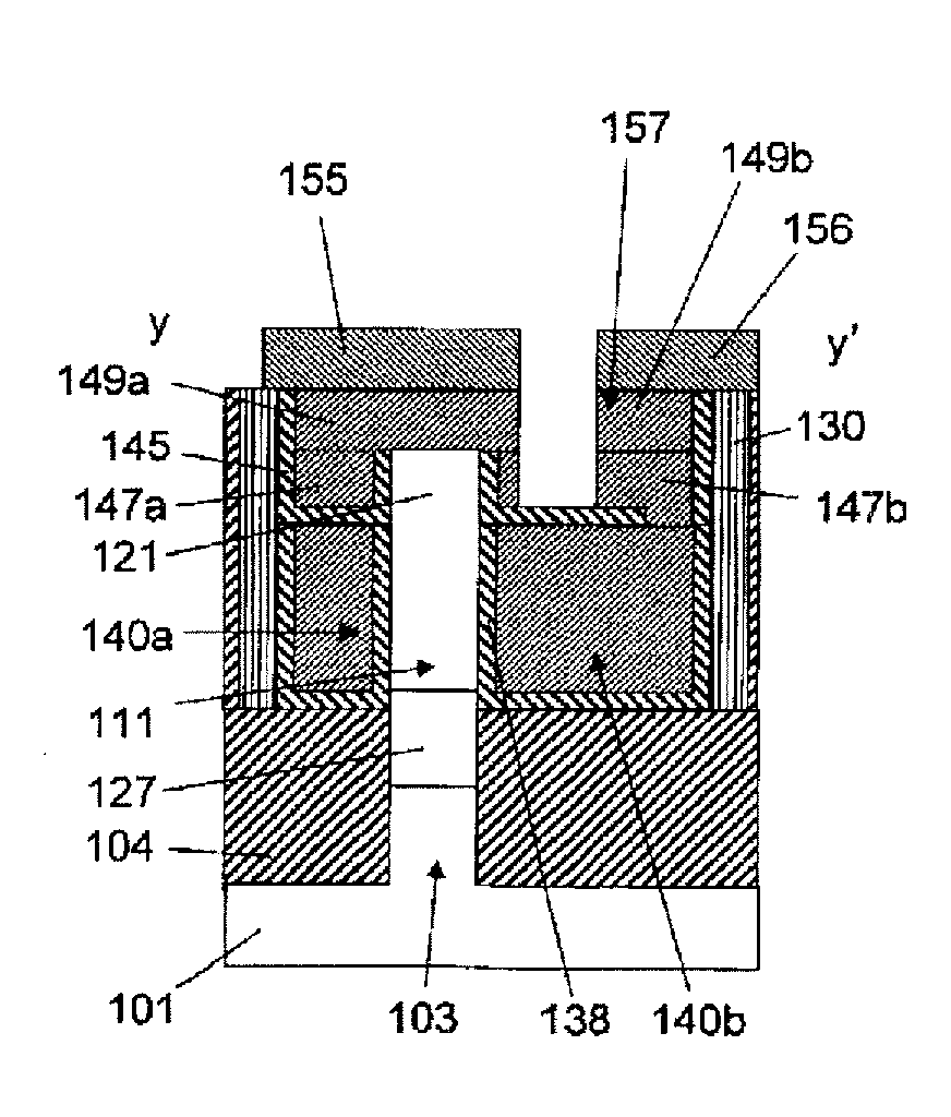
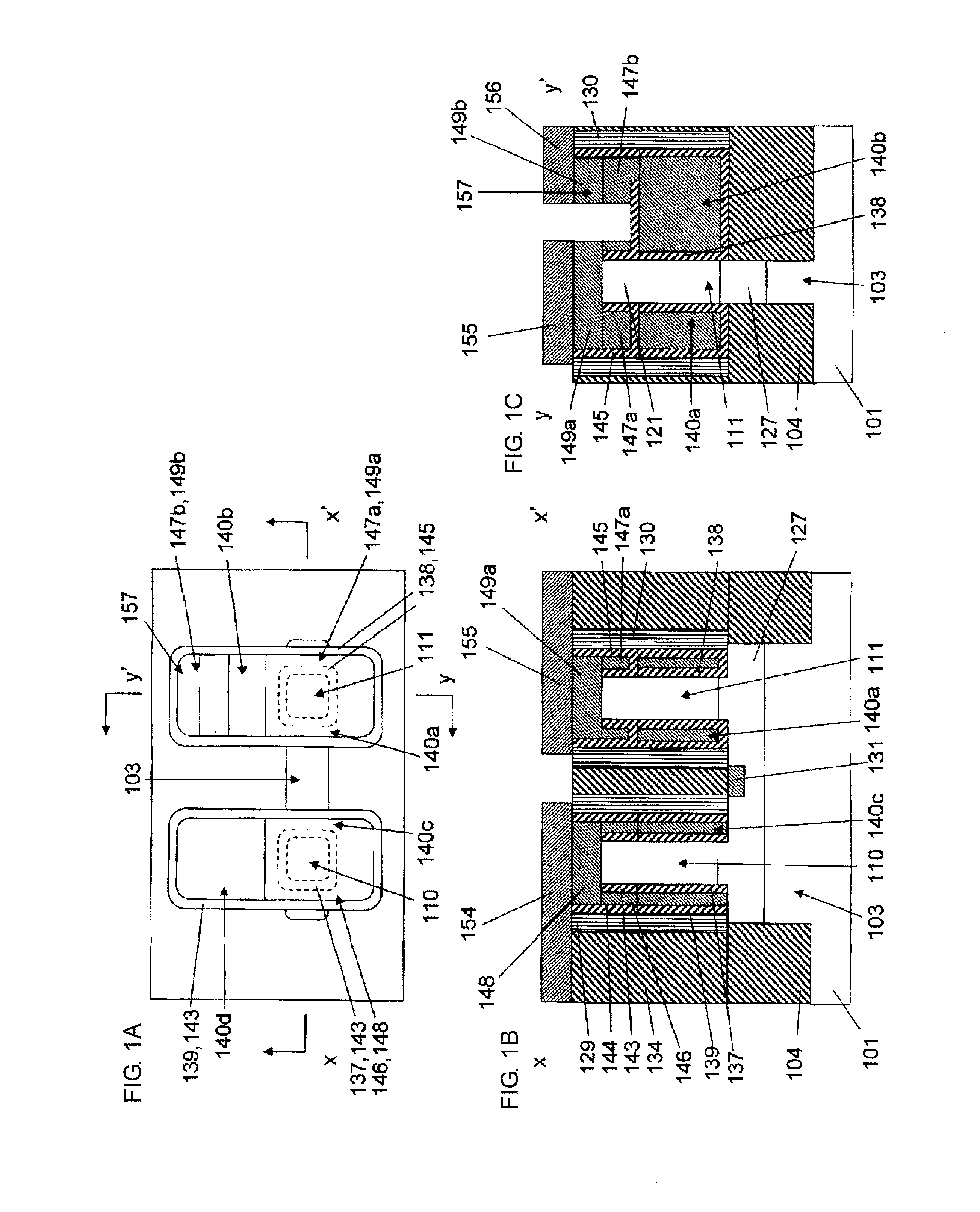
[0082]Hereinafter, production steps for forming an SGT structure according to an embodiment of the present invention will be described with reference to FIGS. 2A to 41C.
[0083]First, the following is a description of a first step of forming a fin-shaped semiconductor layer on a semiconductor substrate and forming a first insulating film around the fin-shaped semiconductor layer. In this embodiment, a silicon substrate is employed; however, another substrate formed of semiconductor may also be used.
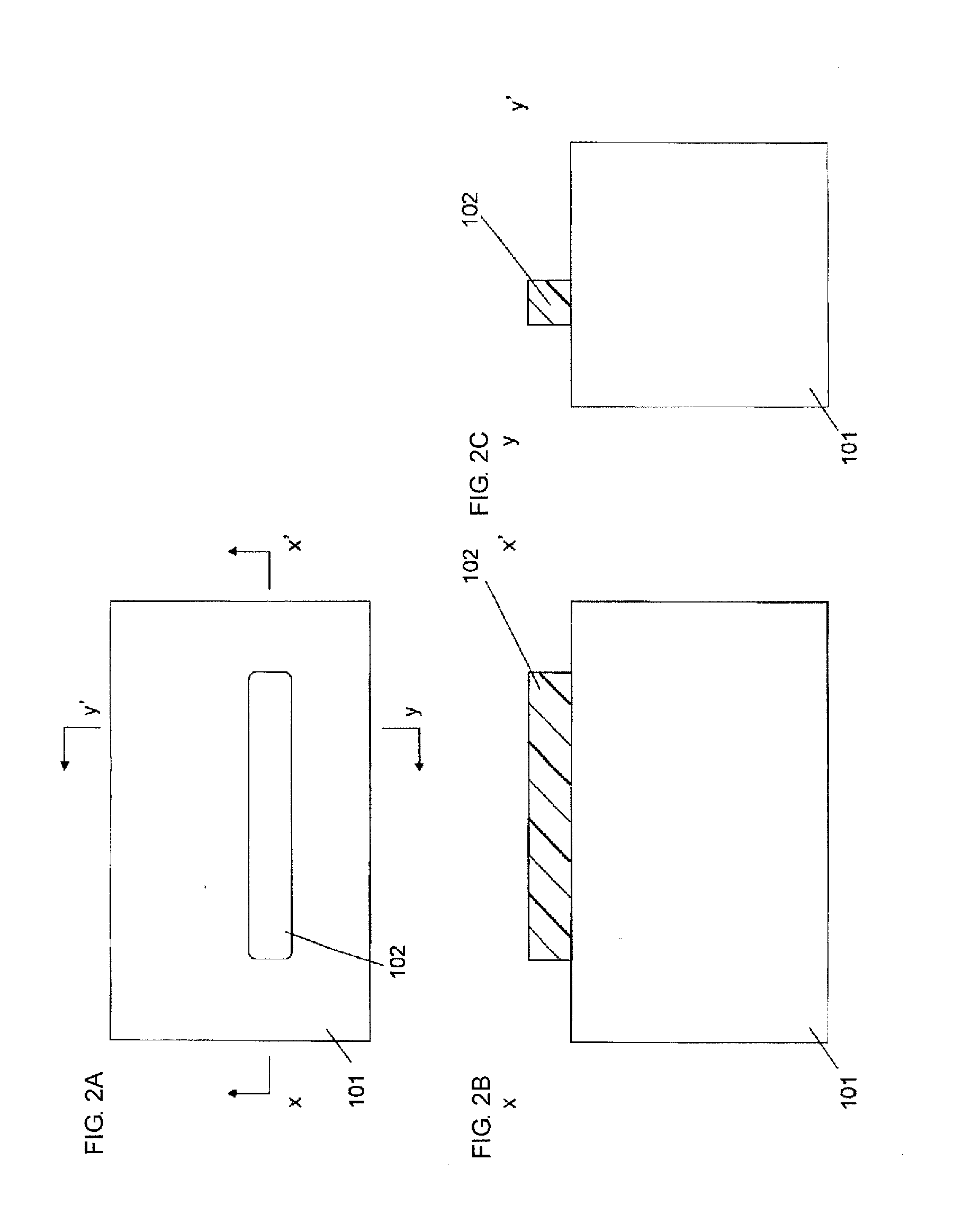
[0084]As illustrated in FIGS. 2A to 2C, a first resist 102 for forming a fin-shaped silicon layer is formed on a silicon substrate 101.
[0085]As illustrated in FIGS. 3A to 3C, the silicon substrate 101 is etched to form a fin-shaped silicon layer 103. In this embodiment, the resist is used as a mask for forming the fin-shaped silicon layer; alternatively, a hard mask such as an oxide film or a nitride film may be used.
[0086]As illustrated in FIGS. 4A to 4C, the first resist 102 is removed.
[0...
PUM
 Abstract
Description
Claims
Application Information