Supercharge Your Innovation With Domain-Expert AI Agents!

Preparation method of patterned film, display substrate and display device

a technology of patterned film and substrate, applied in the field of display, can solve the problems of increasing cost, increasing difficulty in mass production, affecting the quality of products, etc., and achieve the effect of improving product quality and product percent of pass

Active Publication Date: 2015-12-31
BOE TECH GRP CO LTD
View PDF5 Cites 3 Cited by
  • Summary
  • Abstract
  • Description
  • Claims
  • Application Information

AI Technical Summary

Benefits of technology

The present invention provides a method for making a patterned film, a display substrate and a display device. This method avoids the issue of film layer falling off when peeling off a photoresist layer, resulting in improved product quality and higher product pass rate. In simple terms, this method involves forming a preset film layer on a substrate, covering it with an isolation layer, adding a photoresist layer on top, patterning the isolation layer with the photoresist layer, and then removing the preset film layer and remaining isolation layer to create the patterned film.

Problems solved by technology

However, there is an urgent need for alternative materials due to indium being rare metal, a lack of resources, toxic indium oxides, and environmental protection.
However, since the silver nanowire film is relatively thin, falling off of the silver nanowire film or residual of photoresist on the silver nanowires may occur when peeling off by using the current conventional photoresist, thus seriously affecting the quality of products.
Moreover, developing specific photoresist materials and processes for the silver nanowire film will increase costs and increase difficult in mass production.

Method used


Image

  • Preparation method of patterned film, display substrate and display device
  • Preparation method of patterned film, display substrate and display device
  • Preparation method of patterned film, display substrate and display device

Examples


Embodiment Construction

[0021]Technical solutions in the embodiments of the present invention will be clearly and completely described below, by referring to the drawings in the embodiments of the present invention. Obviously, the described embodiments are merely part of the embodiments of the present invention, but not all embodiments. Based on the embodiments of the present invention, all other embodiments obtained by one of ordinary skill in the art without creative efforts, all belong to the protection scope of the present invention.

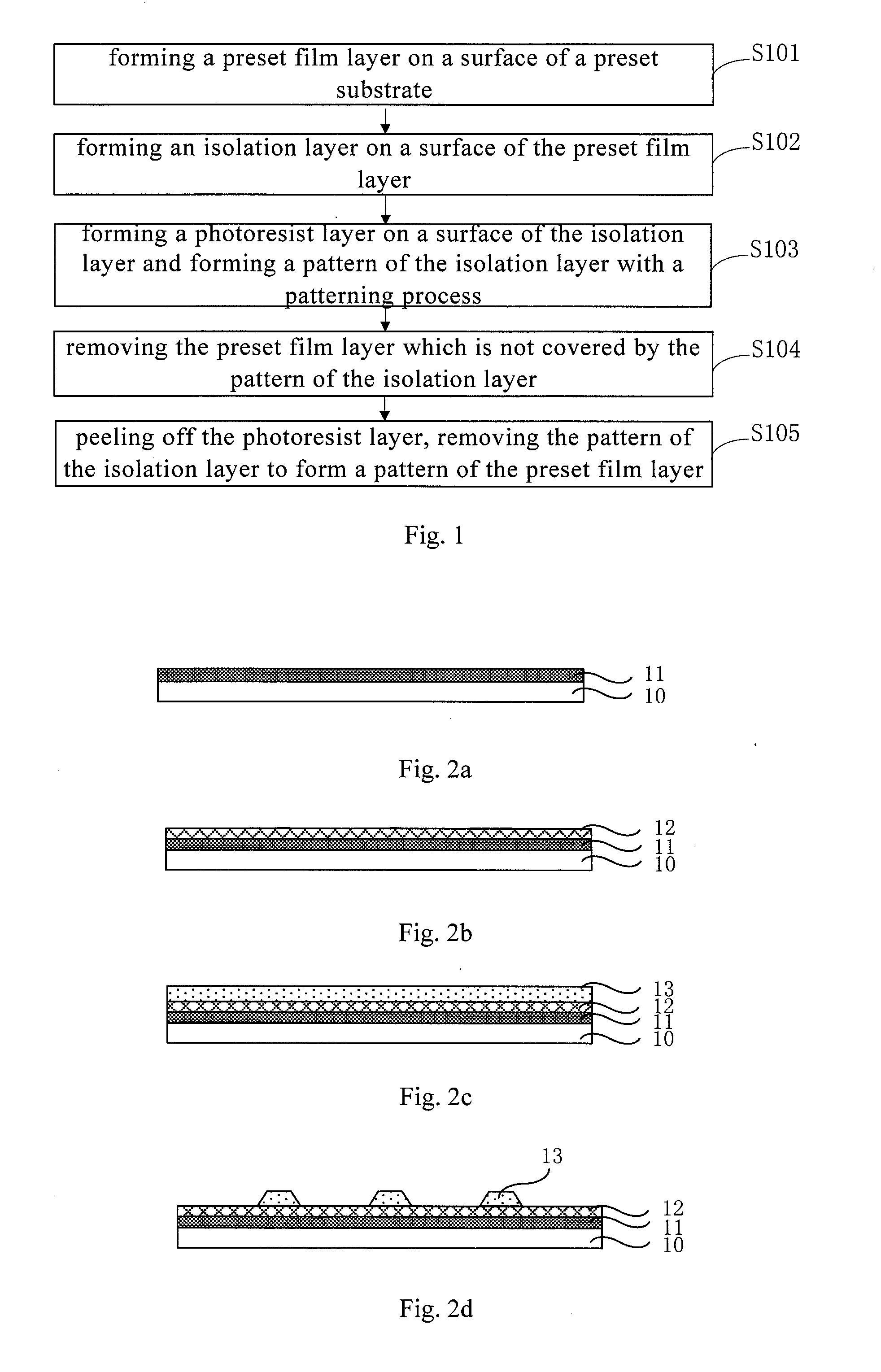
[0022]Embodiments of the present invention provide a preparation method of a patterned film, as shown in FIG. 1, comprising:

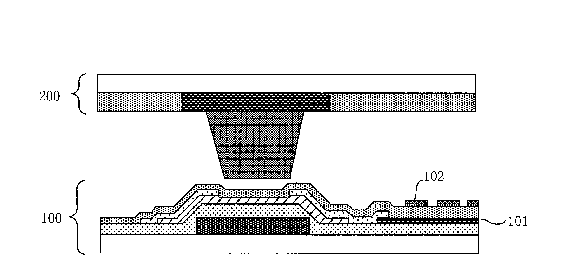
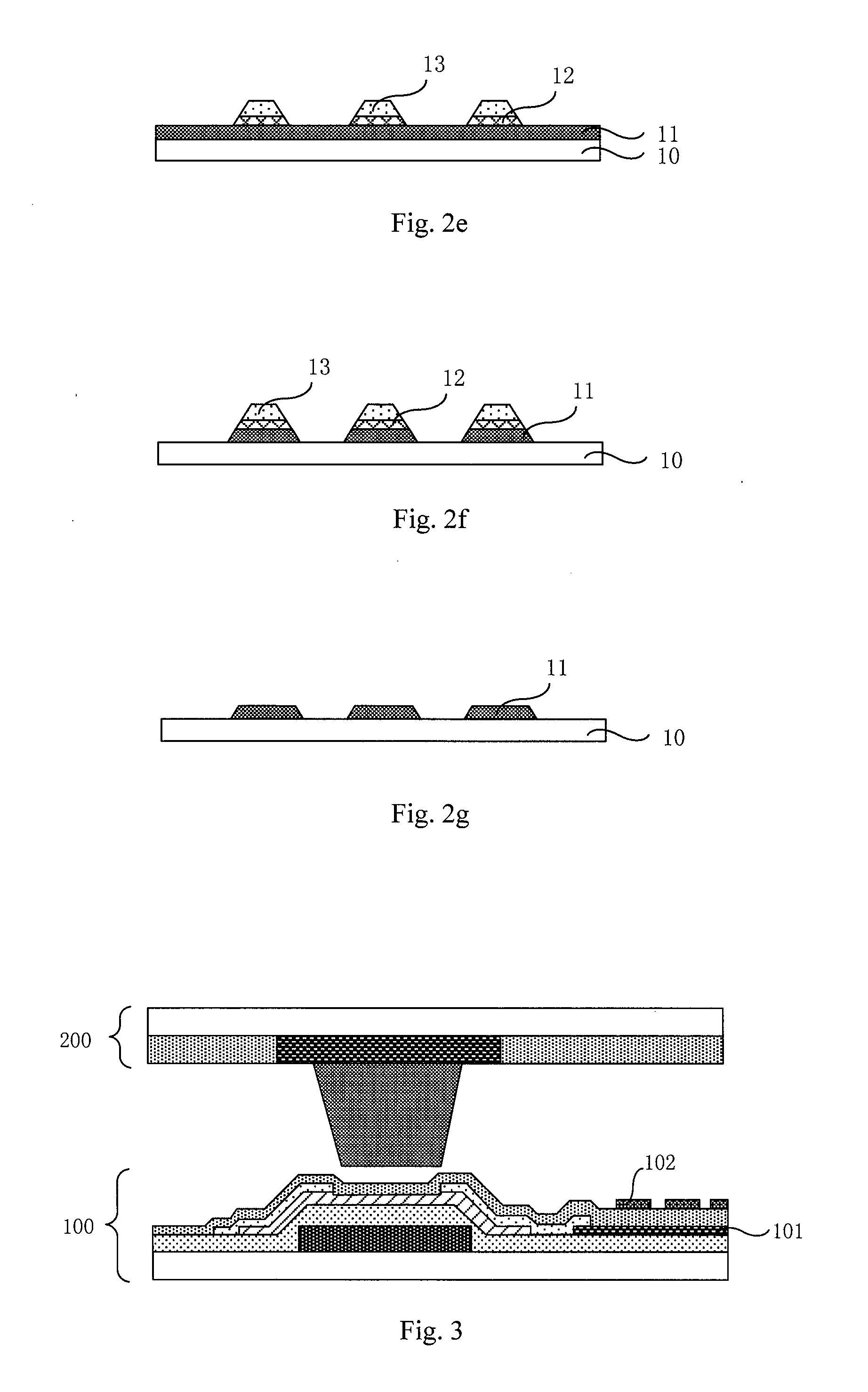
[0023]S101: as shown in FIG. 2a, a preset film layer 11 is formed on a surface of a preset substrate 10.

[0024]It should be noted that the surface of the preset substrate 10 may be a surface of a transparent substrate, or may be the surface of the uppermost film layer in a plurality of film layers formed with a stacked structure on the transparent subst...


PUM


Abstract

Embodiments of the present invention provide a preparation method of a patterned film, a display substrate and a display device, avoiding falling off of a film layer occurring in the process of peeling off a photoresist layer. The preparation method of the patterned film comprises: forming a preset film layer on a surface of a preset substrate; covering the preset film layer with an isolation layer; forming a photoresist layer on a surface of the isolation layer and forming a pattern of the isolation layer with a patterning process; then removing the preset film layer which is not covered by the pattern of the isolation layer, peeling off the photoresist layer and removing the remaining, isolation layer to form a pattern of the preset film layer.

Description

RELATED APPLICATIONS[0001]The present application claims the benefit of Chinese Patent Application No. 201410306505.0, filed Jun. 30, 2014, the entire disclosure of which is incorporated herein by reference.FIELD OF THE INVENTION[0002]The present invention relates to display field, in particular to a preparation method of a patterned film, a display substrate and a display device.BACKGROUND OF THE INVENTION[0003]The transparent conductive film is a conductive film which can be coated on a surface of a substrate with high transmittance. The film has excellent optical transparency and surface conductivity, and is widely used in display field.[0004]In the transparent conductive film, an indium tin oxide (referred to as ITO) film which has excellent optical transparency and conductivity, becomes a material which is most widely used. However, there is an urgent need for alternative materials due to indium being rare metal, a lack of resources, toxic indium oxides, and environmental prote...

Claims


Application Information

Patent Timeline
Patent Type & Authority Applications(United States)
IPC IPC(8): H05K3/06H05K1/02H05K1/09
CPCH05K3/064H05K2201/0108H05K2201/10128H05K1/097H05K3/062H05K2201/026H05K2203/0574
Inventor LI, LINTANG, CHENXIN, YANGYANGCHANG, SHAN
Owner BOE TECH GRP CO LTD
Features
  • R&D
  • Intellectual Property
  • Life Sciences
  • Materials
  • Tech Scout
  • Unparalleled Data Quality
  • Higher Quality Content
  • 60% Fewer Hallucinations
Learn More