Waveguide antenna assembly and system for electronic devices

a technology of electronic devices and antenna assemblies, applied in the direction of antennas, slot antennas, basic electric elements, etc., can solve the problems of coupling and detuning antenna impedance/resonance, gain and bandwidth, and limited wireless electronic device functionality,

Active Publication Date: 2016-01-07
POULSON KIM
View PDF4 Cites 2 Cited by
  • Summary
  • Abstract
  • Description
  • Claims
  • Application Information

AI Technical Summary

Benefits of technology

[0009]As further described below, the conformability of the present waveguide's conductive layer imparts adaptability to diverse shapes and sizes and physical configurations wherein they may be fitted within, around or on variously shaped electronic devices supported thereby. Such conformability enables adaptability to underlying device package redesigns without compromising specificat...

Problems solved by technology

Conventional antenna systems utilizing, for example, wire, PIFA, resonant loop, chip, patch, stripline antennas and other similar traditional antenna configurations have, in the past, limited the functionality of wireless electronic devices due to power loss resulting from inefficiencies, and associated limitations on bandwidth and gain, coupling and detuning antenna impedance/resonance and other limitations perpetuated by antenna systems conventionally employed.
A particular issue with such conventional antenna assemblies arises from antenna coupling with surrounding or adjacent surfaces adversely impacting radiation pattern and input match associated with use of a conventional open body antenna.
Such coupling and detuning issues impose design limita...

Method used


Image

  • Waveguide antenna assembly and system for electronic devices
  • Waveguide antenna assembly and system for electronic devices
  • Waveguide antenna assembly and system for electronic devices

Examples


Embodiment Construction

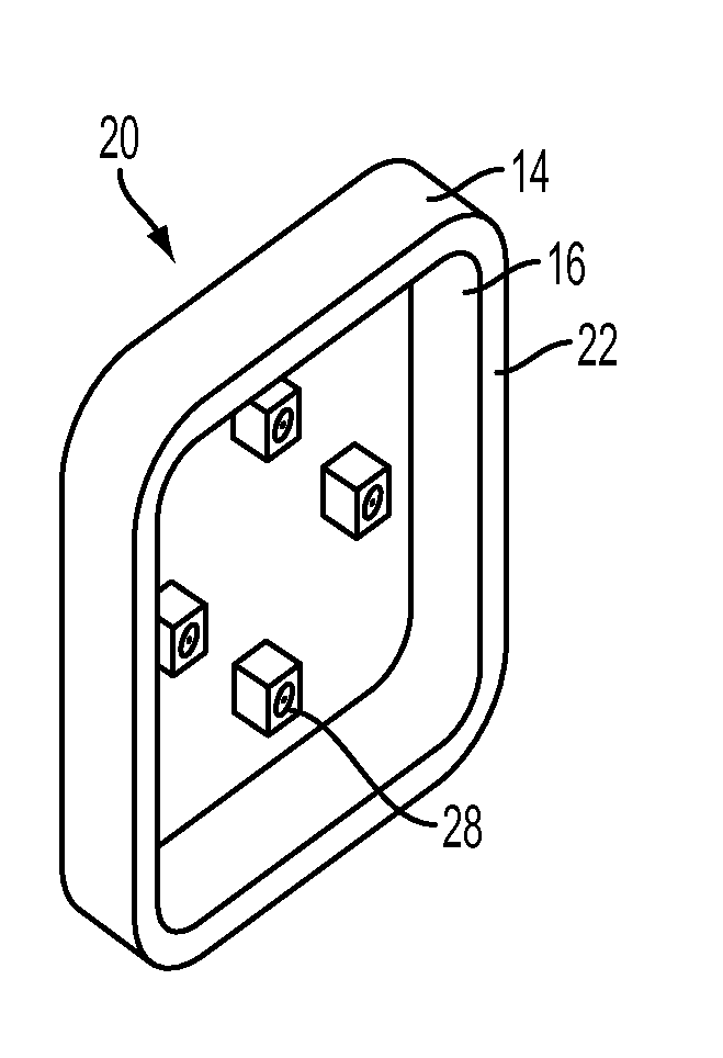
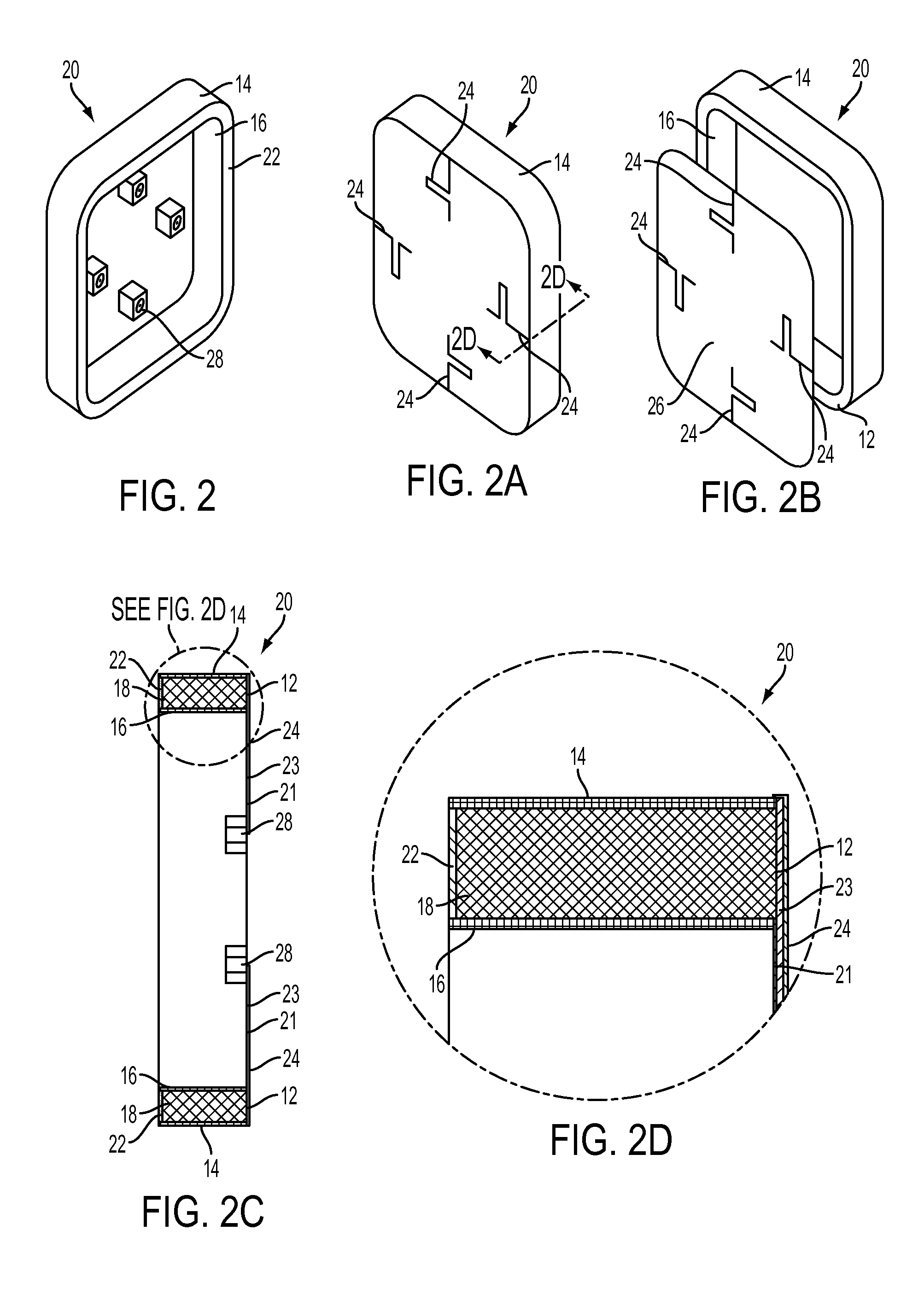
[0034]Referring to the drawings, preferred embodiments and operational details of the present waveguide antenna assembly and system are shown and described in detail. In order to more particularly point out and clearly define the presently claimed invention, particularly spatial orientation and electromagnetic correspondence of components of the waveguide assembly, this paragraph defines terms used herein to describe and claim the present invention. To that end, dimensional arrangements are defined along Cartesian longitudinal and transverse axes. Accordingly, as referred to herein, and well known in the relevant art, a longitudinal direction is parallel to the Cartesian Z axis and the transverse direction parallel to the Cartesian X-Y axis. As illustrated, the X-axis is disposed in a horizontal transverse direction and the Y-axis is disposed in a vertical transverse direction. The term “collateral” as used herein defines spatial orientation electrically conductive layers, claimed a...


PUM


Abstract

A waveguide antenna assembly and process for transceiving signals of a predetermined radio frequency range comprising at least two collaterally aligned conductive layers configured in a conformable loop so as to form an electrically isolating channel dimensionally configured for support of the waveguide modes of the predetermined frequency range, an aperture for electromagnetically transceiving the signals, wherein the aperture extends along a surface of the electrically isolating channel such that the aperture extends between the outer edge of the inner surface of the first conductive layer and the second conductive layer, a back short spaced apart from the aperture a predetermined distance equal to a resonant length of the waveguide mode wavelength so as to provide a circuit impedance between the first conductive layer and the second conductive layer for tuning the waveguide to transceive the signals, and excitation points coupled to the aperture to propagate waveguide modes within the electrically isolating channel, which is conformable to the configuration of a supported electronic device.

Description

CROSS-REFERENCE TO RELATED APPLICATION[0001]This application claims the benefit of U.S. Provisional Patent Application Ser. No. 61 / 998,714 filed on Jul. 7, 2014.FIELD OF THE INVENTION[0002]The present invention relates to antenna assemblies and systems for wireless electronic devices.BACKGROUND OF THE INVENTION[0003]Conventional antenna systems utilizing, for example, wire, PIFA, resonant loop, chip, patch, stripline antennas and other similar traditional antenna configurations have, in the past, limited the functionality of wireless electronic devices due to power loss resulting from inefficiencies, and associated limitations on bandwidth and gain, coupling and detuning antenna impedance / resonance and other limitations perpetuated by antenna systems conventionally employed. A particular issue with such conventional antenna assemblies arises from antenna coupling with surrounding or adjacent surfaces adversely impacting radiation pattern and input match associated with use of a conv...

Claims


Application Information

Patent Timeline
IPC IPC(8): H01Q13/18H01Q13/10
CPCH01Q13/103H01Q13/18
Inventor POULSON, KIM
Owner POULSON KIM
Why Eureka
Try Eureka