Lens array substrate, electro-optical apparatus and electronic equipment

a technology of electrooptical equipment and array substrate, which is applied in the direction of optics, mountings, instruments, etc., can solve the problems of insufficient thickness, difficult to provide the optical path length adjustment layer, and reduce the amount of light contributing to the display

Inactive Publication Date: 2016-01-21
SEIKO EPSON CORP
View PDF2 Cites 10 Cited by
  • Summary
  • Abstract
  • Description
  • Claims
  • Application Information

AI Technical Summary

Benefits of technology

[0010]An advantage of some aspects of the embodiments is to provide a lens array substrate which is capable of preventing the reflection generated on an interface between a lens layer and a translucent layer (an optical path length adjusting layer), an electro-optical apparatus which is provided with the lens array substrate, and electronic equipment which is provided with the electro-optical apparatus.

Problems solved by technology

In the lens array substrate, it is preferable to provide an optical path length adjusting layer (a translucent layer) having a predetermined thickness on the emission side with respect to the lens in order to properly control a position in which the light emitted from a lens is converged; however, the optical path length adjusting layer (the translucent layer) having a sufficient thickness is not provided in the lens array substrate disclosed in JPA-2013-57781.
In addition, in the lens array substrate disclosed in JP-A-2013-57781, since the concave surface on which the first lens surface is reflected is used as the second lens surface for the surface opposite to the side of the translucent substrate in the first lens layer, it is difficult to provide the optical path length adjusting layer (the translucent layer) having the sufficient thickness with respect to the first lens surface.
However, in the above-described configuration, there is a problem in that a reflection is generated on an interface between the first lens layer which is formed of the silicon oxinitride film and the first translucent layer which is formed of the silicon oxide film, or an interface between the first translucent layer which is formed of the silicon oxide film and the second lens layer which is formed of the silicon oxinitride film, and therefore, it is likely that an amount of light contributing to a display will be reduced.

Method used


Image

  • Lens array substrate, electro-optical apparatus and electronic equipment
  • Lens array substrate, electro-optical apparatus and electronic equipment
  • Lens array substrate, electro-optical apparatus and electronic equipment

Examples


first embodiment

Configuration of Electro-Optical Apparatus

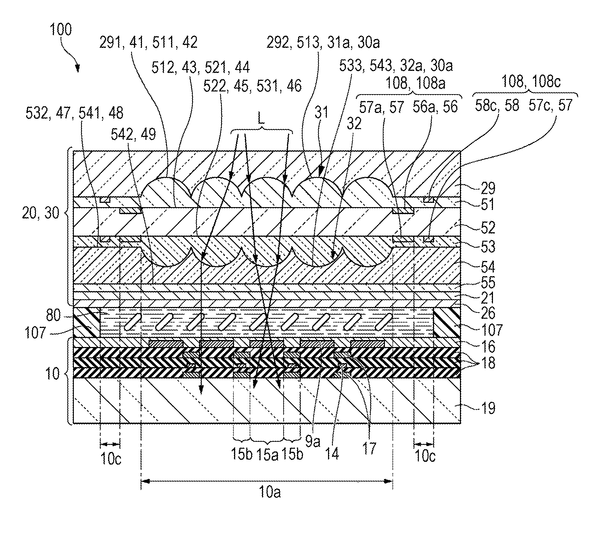
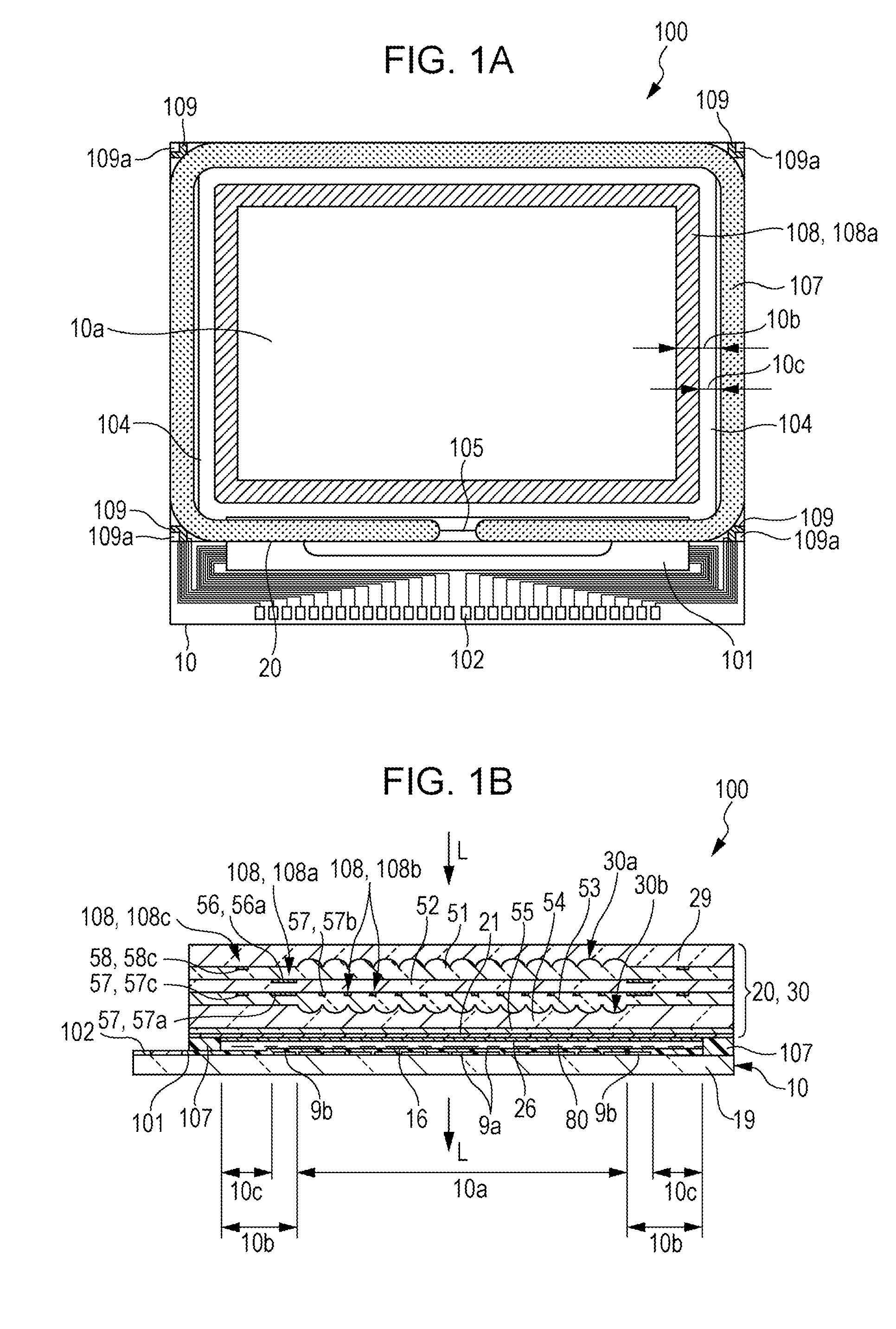
[0038]FIG. 1A and FIG. 1B are illustrative diagrams of an electro-optical apparatus 100 according to the first embodiment, FIG. 1A and FIG. 1B are respectively a plan view of the electro-optical apparatus 100 to which the first embodiment of the invention is applied when seen from the side of each of the component and a counter substrate, and a sectional view thereof.

[0039]As illustrated in FIG. 1A and FIG. 1B, in the electro-optical apparatus 100, a translucent element substrate 10 and a translucent counter substrate 20 are attached to each other with a predetermined interval therebetween by using a sealant 107, and the element substrate 10 and the counter substrate 20 face each other. The sealant 107 is formed into a frame shape so as to be arranged along an outer edge of the counter substrate 20, and an electro-optical layer 80 which is formed of a liquid crystal layer is disposed in the area which is surrounded by the sealant 107 between...

modification example of first embodiment

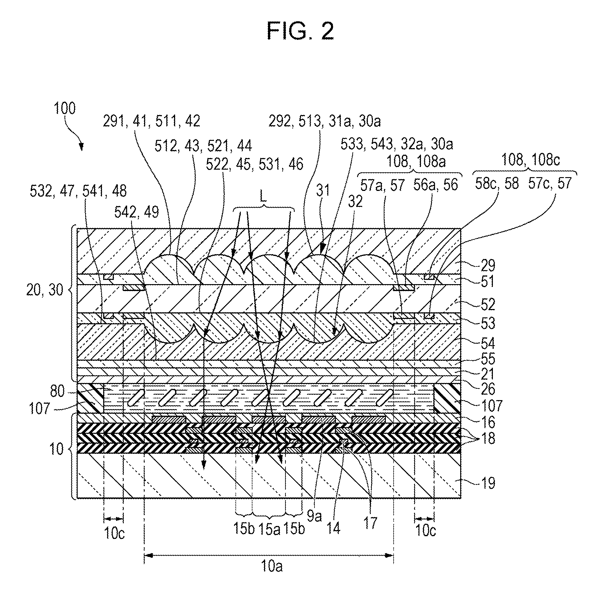
[0109]In the first embodiment as described above, the first lens surface is formed of the first concavity 292, but the invention may be applied to a case where the first lens surface which is formed into the convex surface (the convexity) is formed on the translucent substrate. In addition, the second convexity 533 (the second lens surface) is formed on the second lens layer 53; however, the invention may be applied to a case where the concave surface (the second lens surface) is formed on the second lens layer 53, instead of the second convexity 533.

[0110]In addition, in a case where the first metal layer 56 is not provided between the first lens layer 51 and the first translucent layer 52, the first lens layer 51 and the first translucent layer 52 may be formed in succession, and in a case where the second metal layer 57 is not provided between the first translucent layer 52 and the second lens layer 53, the first translucent layer 52 and the second lens layer 53 may be formed in ...

second embodiment

Modification of Second Embodiment

[0138]In the second embodiment as described above, the lens surface is formed of the first concavity 292, but the invention may be applied to a case where the convexity (the lens surface) which is formed into the convex surface is formed on the translucent substrate.

[0139]In the second embodiment as described above, when it comes to forming the parting 108a, a portion of the first metal layer 56 (the parting 56a) was used, but the parting 108a may be formed by using only a portion of the third metal layer 58.

Application Examples of Other Electro-Optical Apparatuses

[0140]In the above-described embodiments, the liquid crystal device was described as an example of the electro-optical apparatus; however, the invention is not limited thereto, and may be applied to an electro optical module using an organic electroluminescent display panel, a plasma display panel, a field emission display (FED) panel, a surface-conduction electron-emitter display (SED) pan...


PUM

PropertyMeasurementUnit
refractive indexaaaaaaaaaa

Abstract

When it comes to configuring the lens array substrate on which a multistage lens array is formed, a first concavity which is formed of the concave surface is formed on a first surface which is formed of a substrate surface of one of several translucent substrates. In addition, on the substrate surface of one of the translucent substrates, a first lens layer, a first translucent layer, a second lens layer, a second translucent layer, a translucent protective layer, and a common electrode are stacked in order. The first translucent layer has the same refractive index as that of the first lens layer and the second lens layer. In addition, a refractive index of the protective layer is within a range between the refractive index of the second translucent layer and the refractive index of the common electrode.

Description

BACKGROUND[0001]1. Technical Field[0002]The present invention relates to a lens array substrate on which a lens is formed, an electro-optical apparatus which is provided with the lens array substrate, and electronic equipment which is provided with the electro-optical apparatus.[0003]2. Related Art[0004]In a display area of an electro-optical apparatus (a liquid crystal device) which is used as a light valve of a projector, a plurality of pixels are disposed in a matrix shape, and in the pixel, only the light which reaches a translucent area (a pixel opening area) surrounded by a wiring or the like is imparted to display. Here, a configuration such that light from a lighting source is converged to a translucent area by configuring the electro-optical apparatus with a lens array substrate as a counter substrate has been proposed. In addition, as the lens array substrate, a configuration has been proposed such that after a first lens surface which is formed of a concave surface is for...

Claims


Application Information

Patent Timeline
Patent Type & Authority Applications(United States)
IPC IPC(8): G02B3/00G02F1/1335
CPCG02B3/0068G02F1/133526G02B3/0056G02F1/133502G02F1/133512
Inventor ITO, SATOSHINAKAGAWA, MASASHIOIKAWA, HIROYUKI
Owner SEIKO EPSON CORP
Why Eureka
Try Eureka