Method for etching piezoelectric film and method for manufacturing piezoelectric element

a piezoelectric film and piezoelectric element technology, applied in piezoelectric/electrostrictive/magnetostrictive devices, piezoelectric/electrostrictive device manufacture/assembly, electrical apparatus, etc., can solve the problems of poor adhesion between resist and pzt, high cost, and residue left during etching in non-epitaxial pzt films. achieve the effect of high accuracy

Active Publication Date: 2016-01-28
FUJIFILM CORP
View PDF4 Cites 12 Cited by
  • Summary
  • Abstract
  • Description
  • Claims
  • Application Information

AI Technical Summary

Benefits of technology

[0039]By using the method for etching a piezoelectric film and the method for manufacturing a piezoelectric element according to the present inven

Problems solved by technology

However, since an expensive apparatus and a long period of time are required for the dry etching, the cost is high.
The etching method described in JP4665025B has a problem in that a residue remains during etching in a non-epitaxial PZT film in which a noble metal electrode is formed on a Si substrate or in a non-epitaxial PZT film to which Nb is added.
In addition, the adhesion between a resist and PZT is poor, the side etching of a PZT film progresses, and the PZT film becomes tapered.
In JP3201251B, the etching is performed through the two steps, and thus there is a problem in tha

Method used


Image

  • Method for etching piezoelectric film and method for manufacturing piezoelectric element
  • Method for etching piezoelectric film and method for manufacturing piezoelectric element
  • Method for etching piezoelectric film and method for manufacturing piezoelectric element

Examples


first embodiment

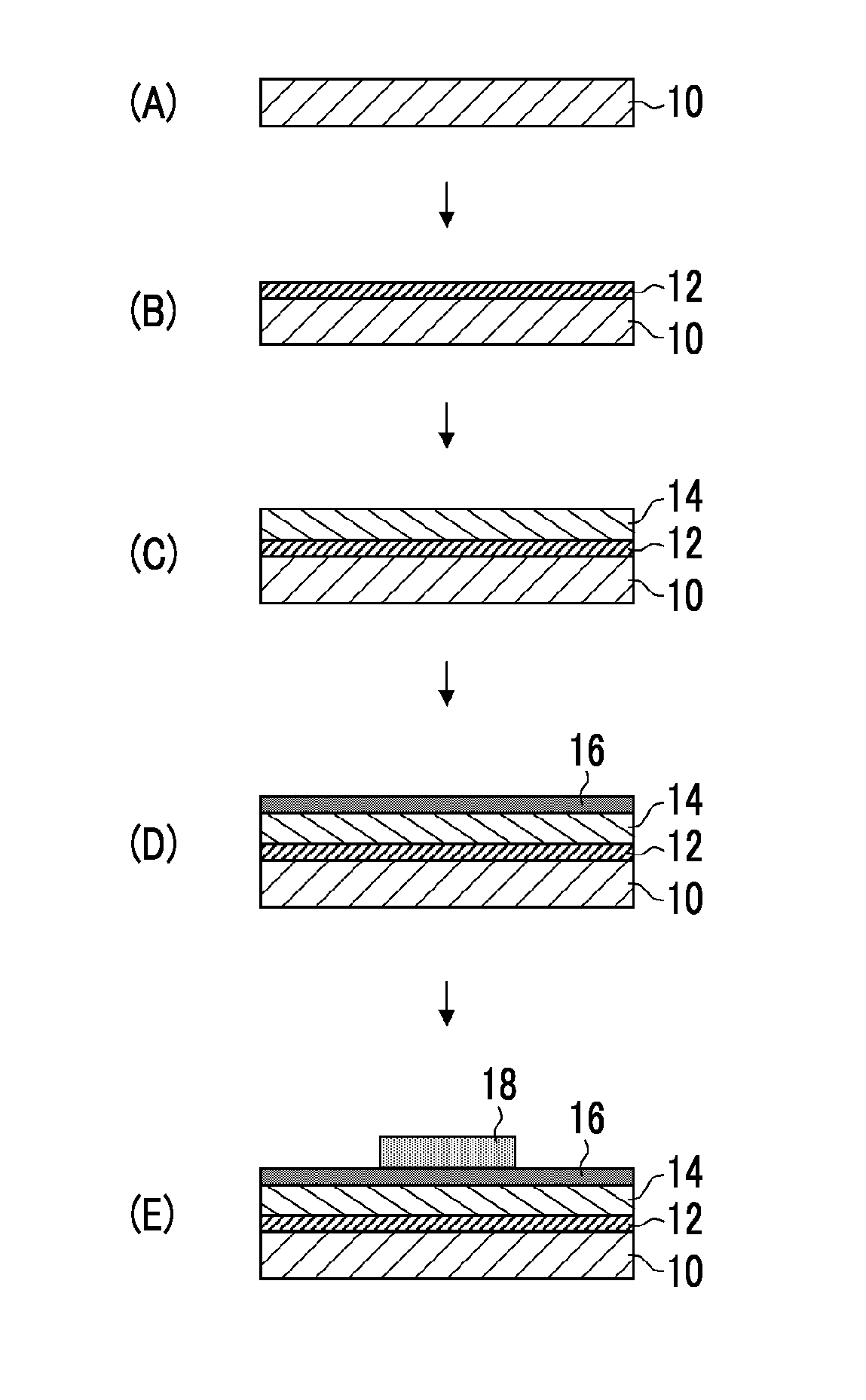
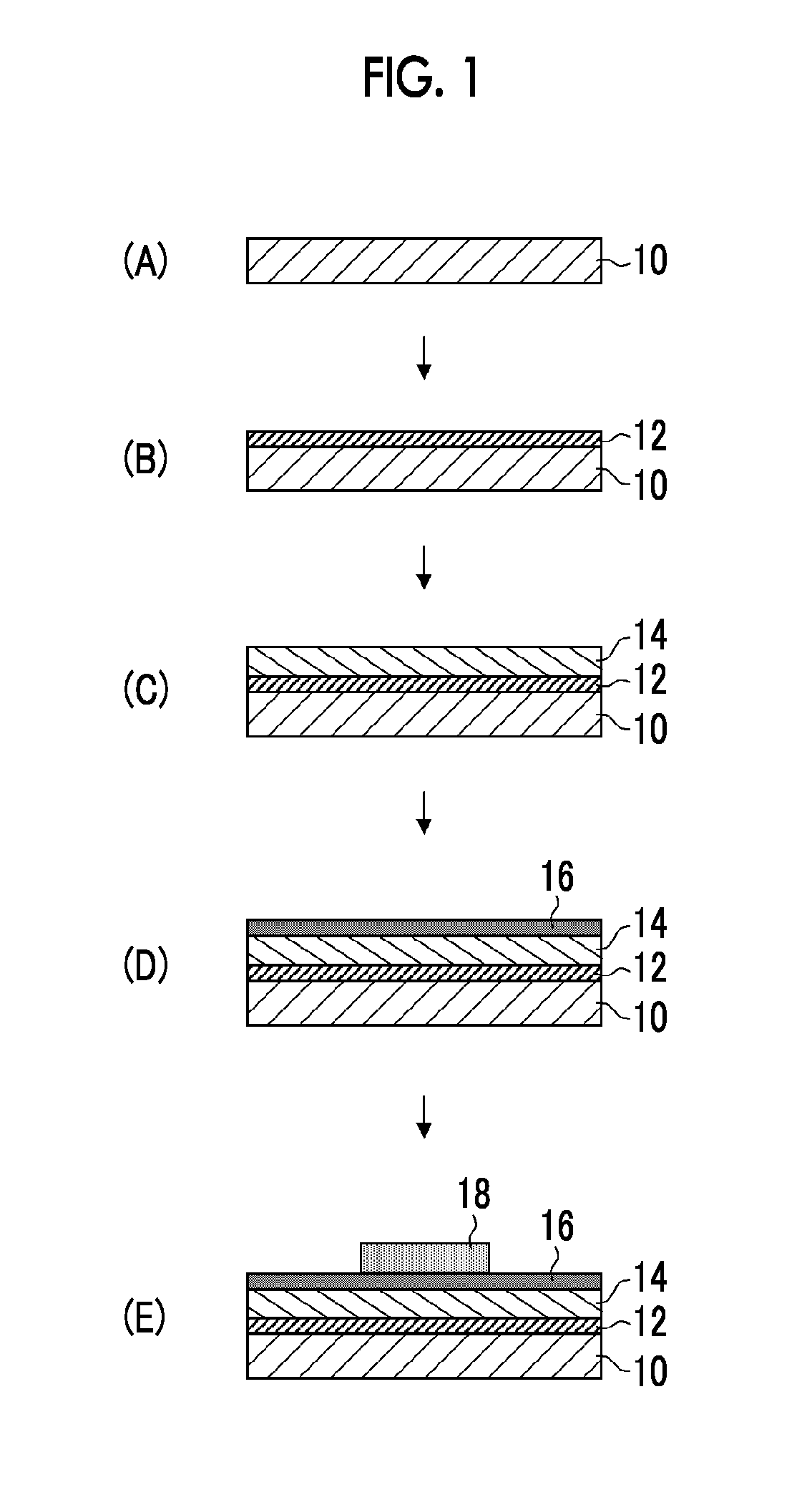
[0051]First, a method for manufacturing a piezoelectric element will be described. FIGS. 1 and 2 are diagrams showing manufacturing steps of a piezoelectric element.

[0052](Step 1: Substrate Preparation Step)

[0053]First, as shown in (A) of FIG. 1, a substrate 10 is prepared.

[0054]The substrate 10 is not particularly limited, and examples thereof include substrates formed of silicon, glass, stainless steel (SUS), yttrium-stabilized zirconia (YSZ), SrTiO3, alumina, sapphire, silicon carbide, and the like. The substrate 10 may be a laminated substrate such as a silicon on insulator (SOI) substrate in which a SiO2 film and a Si active layer are sequentially laminated on a silicon substrate. In addition, for example, a buffer layer for improving lattice matching properties or an adhesion layer for improving adhesion between the electrode and the substrate may be provided between the substrate 10 and the lower electrode 12.

[0055](Step 2): Lower Electrode Forming Step

[0056]Next, a lower ele...

second embodiment

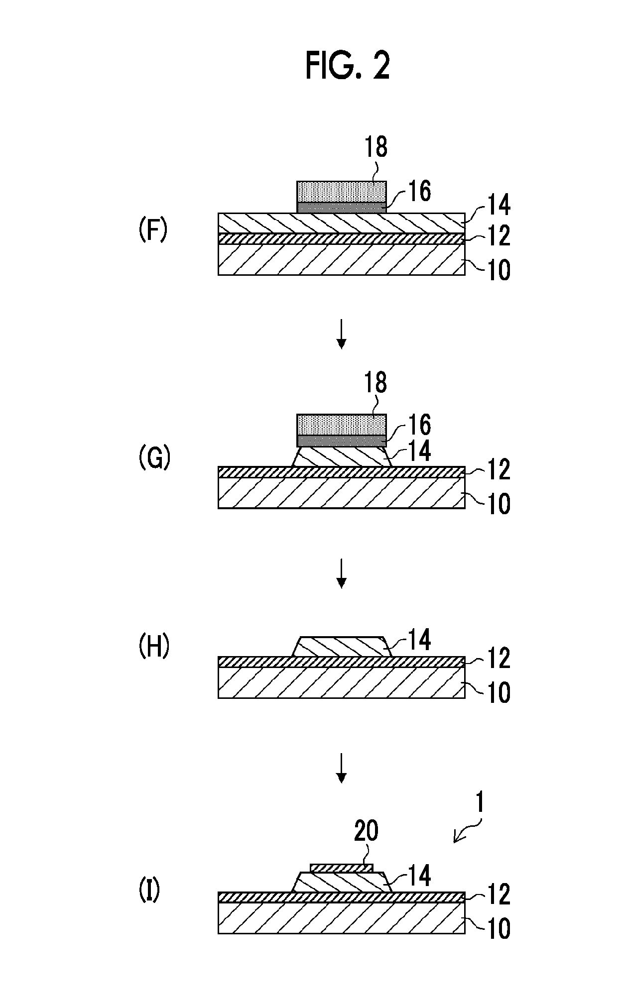
[0127]In the first embodiment, the resist film and the metal film are peeled off after the etching of the piezoelectric film, and then the upper electrode is formed, thereby forming a piezoelectric element. However, a second embodiment is different from the first embodiment, in that the metal film is used as the upper electrode after the resist film is peeled off, thereby forming a piezoelectric element.

[0128]The second embodiment can be performed using the same method as in (Step 1): substrate preparation step to (Step 8): resist film removing step of the first embodiment. In addition, since the metal film 16 functions as an upper electrode, a NiCr alloy, Ni, Cr, Cu, or Au can be used as the material of the metal film.

[0129]In addition, when the upper electrode includes two or more metal films, the respective metal films can be individually formed and etched to manufacture a piezoelectric element. FIG. 4 is a diagram showing a method for manufacturing a piezoelectric element accord...


PUM


Abstract

In a method for etching a piezoelectric film and a manufacturing method thereof, a piezoelectric film is formed on a substrate on which a lower electrode is formed, a metal film having a thickness of 20 nm to 300 nm is formed, a patterned resist film is formed, the metal film is etched with a first etchant to which the piezoelectric film has etching resistance, and the piezoelectric film is etched with a second etchant to which the metal film has etching resistance.

Description

CROSS-REFERENCE TO RELATED APPLICATIONS[0001]The present application is a Continuation of PCT International Application No. PCT / JP2014 / 059123 filed on Mar. 28, 2014 claiming priority under 35 U.S.C §119(a) to Japanese Patent Application No. 2013-076021 filed on Apr. 1, 2013. Each of the above applications is hereby expressly incorporated by reference, in their entirety, into the present application.BACKGROUND OF THE INVENTION[0002]1. Field of the Invention[0003]The present invention relates to a method for etching a piezoelectric film and a method for manufacturing a piezoelectric element and, in particular, relates to a method for etching a piezoelectric film and a method for manufacturing a piezoelectric element, in which the etching is performed by wet etching.[0004]2. Description of the Related Art[0005]A piezoelectric element formed of a piezoelectric material which expands and contracts in response to an increase and decrease in electric field application intensity is used as ...

Claims


Application Information

Patent Timeline
IPC IPC(8): H01L41/332H01L41/29
CPCH01L41/29H01L41/332H10N30/8548H10N30/8554H10N30/06H10N30/082H10N30/877
Inventor FUJII, TAKAMICHIMUKAIYAMA, AKIHIRO
Owner FUJIFILM CORP
Why Eureka
Try Eureka