Silicon-embedded copper nanostructure network for high energy storage

a nanostructure network and copper nanotechnology, applied in the field of lithium ion battery electrodes, can solve the problem of difficult silicon cycling and other problems

Active Publication Date: 2016-01-28
AMPRIUS TECH INC
View PDF0 Cites 10 Cited by
  • Summary
  • Abstract
  • Description
  • Claims
  • Application Information

AI Technical Summary

Problems solved by technology
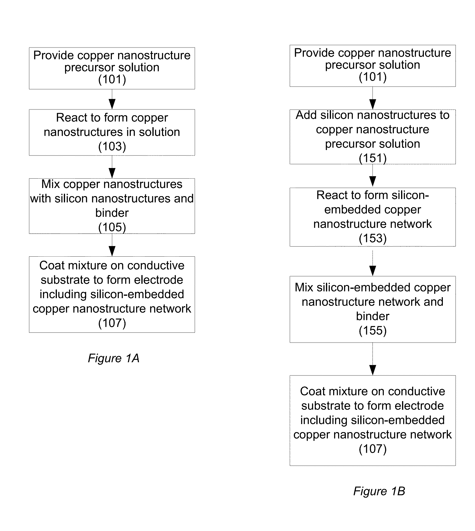
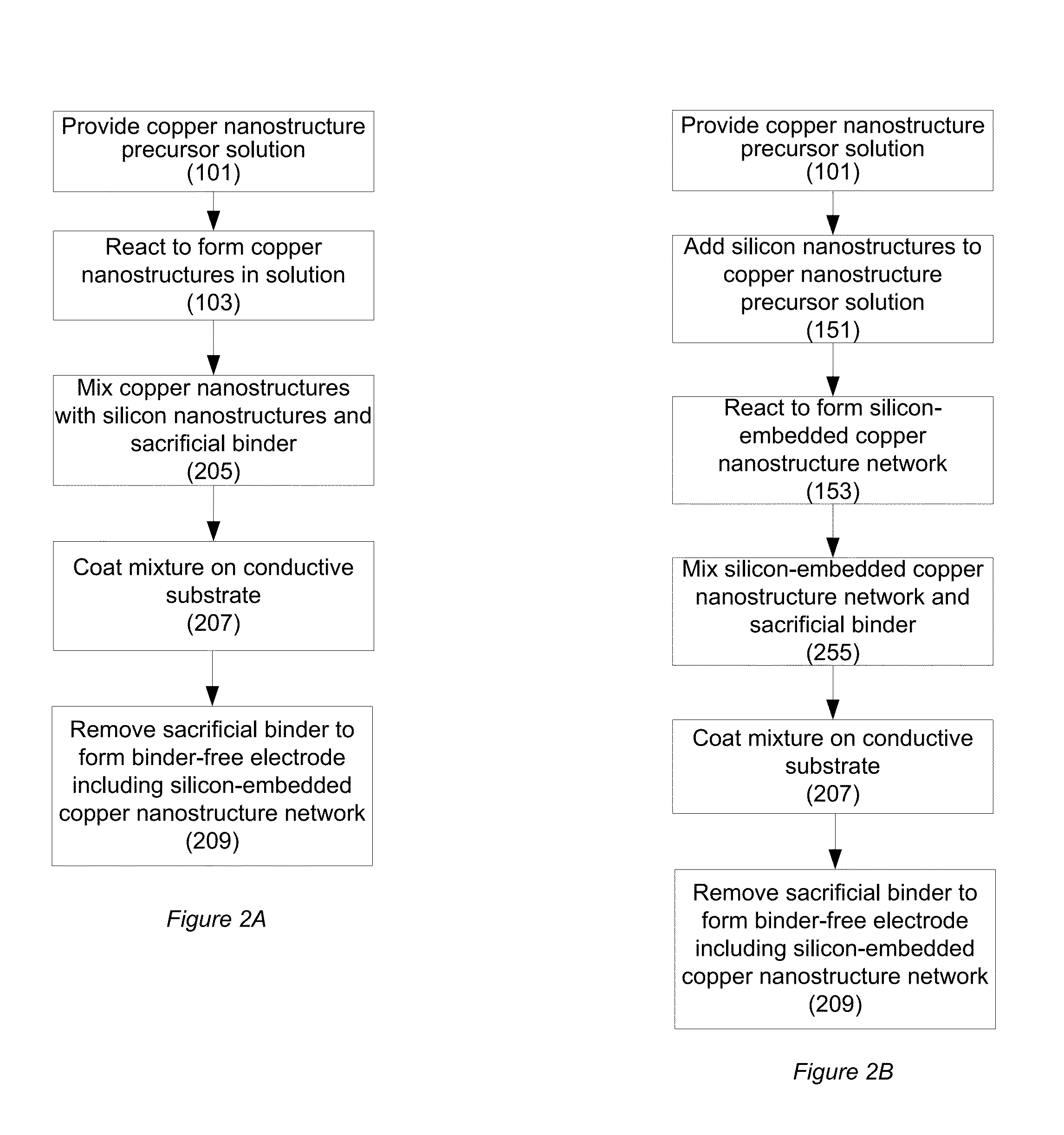
There is a continuous challenge to design lithium batteries with higher and higher energy densities.
However, silicon expands as much as 400% upon lithiation, which causes problems such as cracking, making it difficult for silicon to endure much cycling.
It remains a challenge to exploit the theoretical lithium capacity of silicon in a lithium battery anode.

Method used


Image

  • Silicon-embedded copper nanostructure network for high energy storage
  • Silicon-embedded copper nanostructure network for high energy storage
  • Silicon-embedded copper nanostructure network for high energy storage

Examples


example 1

[0053]Copper nanowires were formed from a solution of 21 mg CuCl2.H2O, 180 mg HDA and 50 mg glucose. The reaction was run at 95° C. for 8 hours. Samples were then taken and dried overnight. FIG. 8 shows SEM images 850 and 852 of a sample at different magnifications. Image 852 shows a very long and flexible copper nanowire. The nanowire 853 was measured at almost 30 microns long, with longer nanowires observed.

example 2

[0054]Copper nanowires were formed as in Example 1 with 270 g HDA (HDA:Cu ratio of 9:1). FIG. 9 shows an SEM image of a sample of a network of nanowires. Diameters of five nanowires were measured, ranging from 31.26 nm to 54.16 nm, with an average value of 39+ / −9 nm.

example 3

[0055]Copper nanowires were formed as in Example 1 with silicon nanoparticle powder added to the solution in a 1:1 Cu:Si molar ratio. Energy-dispersive X-ray spectroscopy (EDS) analysis on two samples gave the following atomic percentages.

Si %Cu %Sample 13466Sample 24555

[0056]Copper was found present in nanowire and nanocrystal forms. Without being bound by a particular theory, it is believed that the large surface area may accelerate copper nucleation and that the amine adsorption on the silicon surface may affect the capping efficiency of the copper crystals.


PUM

PropertyMeasurementUnit
porosityaaaaaaaaaa
porosityaaaaaaaaaa
diametersaaaaaaaaaa

Abstract

Provided herein are nanostructure networks having high energy storage, electrochemically active electrode materials including nanostructure networks having high energy storage, as well as electrodes and batteries including the nanostructure networks having high energy storage. According to various implementations, the nanostructure networks have high energy density as well as long cycle life. In some implementations, the nanostructure networks include a conductive network embedded with electrochemically active material. In some implementations, silicon is used as the electrochemically active material. The conductive network may be a metal network such as a copper nanostructure network. Methods of manufacturing the nanostructure networks and electrodes are provided. In some implementations, metal nanostructures can be synthesized in a solution that contains silicon powder to make a composite network structure that contains both. The metal nanostructure growth can nucleate in solution and on silicon nanostructure surfaces.

Description

CROSS-REFERENCE TO RELATED APPLICATION[0001]This application claims benefit of priority under 35 USC §119(e) to U.S. Provisional Patent Application No. 61 / 813,175, filed Apr. 17, 2013, which is incorporated by reference herein in its entirety.STATEMENT OF GOVERNMENT SUPPORT[0002]The invention described and claimed herein was made in part utilizing funds supplied by the U.S. Department of Energy under Contract No. DE-EE0005474. The Government has certain rights in this invention.FIELD OF THE INVENTION[0003]This invention relates generally to electrodes for lithium ion batteries.BACKGROUND OF THE INVENTION[0004]There is a continuous challenge to design lithium batteries with higher and higher energy densities. Silicon, alone or in combination with other materials such as germanium, tin, antimony and aluminum, has been widely studied as an anode material for lithium batteries. Currently-used graphite anodes have a much lower lithium storage capacity than do silicon anodes. However, sil...

Claims


Application Information

Patent Timeline
Patent Type & Authority Applications(United States)
IPC IPC(8): H01M4/36H01M4/134H01M4/38
CPCH01M4/366H01M4/38H01M2004/021H01M4/386H01M4/134B82Y30/00H01M4/1395H01M4/622H01M4/624H01M4/626H01M10/052Y02E60/10H01M4/387H01M4/483H01M10/0525
Inventor YU, TIANYUE
Owner AMPRIUS TECH INC
Why Eureka
Try Eureka