Scan Speed Optimization of Input and Output Paths

Active Publication Date: 2016-02-04
ADVANTEST CORP
View PDF4 Cites 1 Cited by
  • Summary
  • Abstract
  • Description
  • Claims
  • Application Information

AI Technical Summary

Benefits of technology

The patent describes a system and method for improving the timing and frequency of scanning in a device testing system. By adjusting the timing and frequency of stimulating signals and optimizing the placement of data edges, the system can achieve more efficient data transfer and improve the speed and accuracy of testing. This results in quicker and more reliable device testing.

Problems solved by technology

The ATE input / output timing in current technology generally is a significant limitation on the scan test speeds.
Increasing the scan speed beyond a safe timing margin can cause instability in scan test results.

Method used


Image

  • Scan Speed Optimization of Input and Output Paths
  • Scan Speed Optimization of Input and Output Paths
  • Scan Speed Optimization of Input and Output Paths

Examples


Embodiment Construction

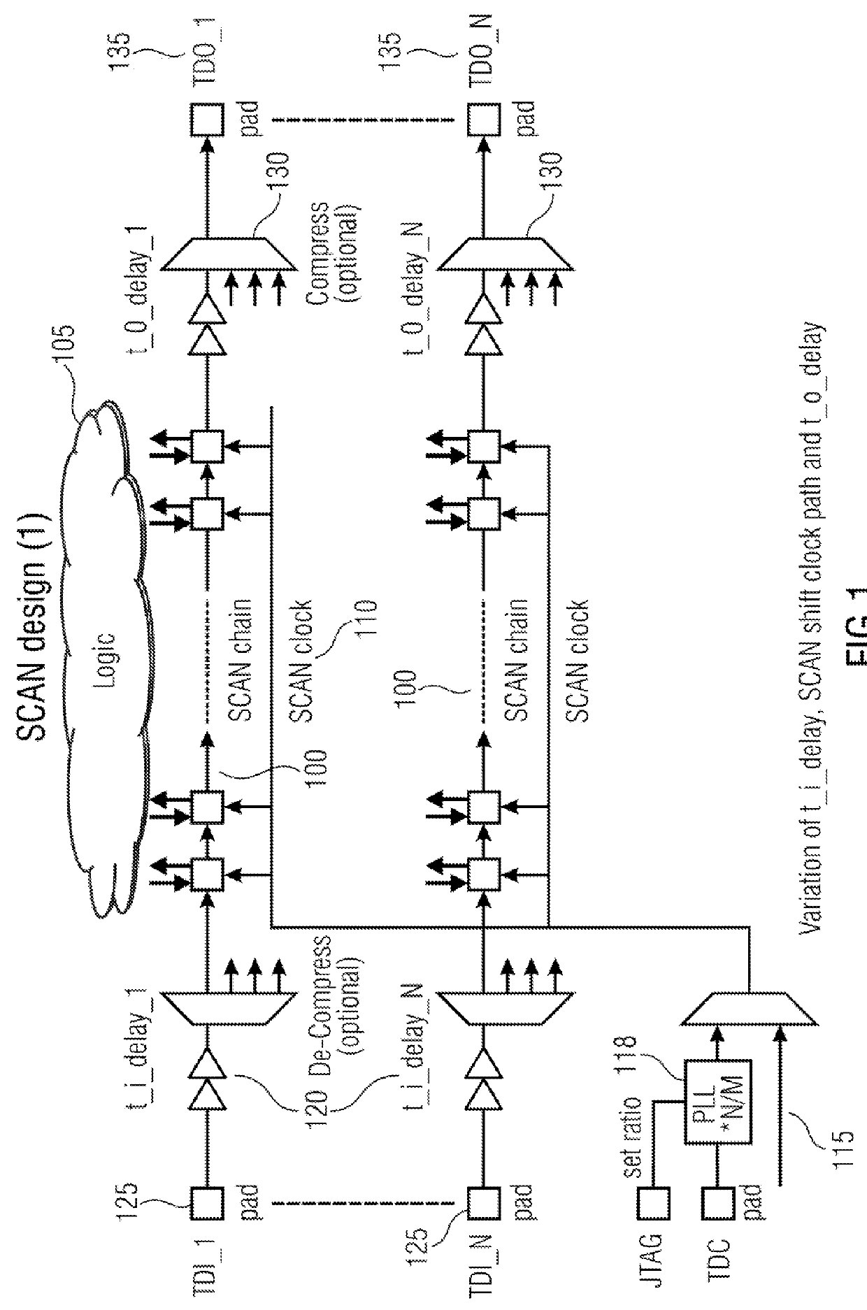
[0041]The system and method disclosed herein addresses optimization of input / output timing for multiple parallel scan chains (although aspects of the invention can be applied to single scan chain design). Note that maximizing frequency takes all of the above-listed factors into account in addition to I / O timing. The input (TDI) and output (TDO) timing is optimized on a per-pin basis. The output timing is adjusted according to the output strobe timing, whereas the input timing is optimized according to the input data edge, which is dependent on the set-up and hold times of the first flip-flop in the chain, as well as path delays. Also note that the maximum attainable frequency is not necessarily the optimum frequency. In practice the optimal operating frequency may be backed off somewhat from the maximum.

[0042]FIG. 1 illustrates the components of an exemplary scan chain system design which involves timing optimization. Scan chains I-N (100) are each coupled to logic 105 and controlle...


PUM


Abstract

Disclosed herein is a scan optimizer system and method designed to generate optimal ATE input / output timing with small margin but yielding stable results. Therefore the scan test time is greatly improved.

Description

CROSS-REFERENCE TO RELATED APPLICATIONS[0001]This application is a continuation of copending International Application No. PCT / EP2013 / 057713, filed Apr. 12, 2013, which is incorporated herein by reference in its entirety.[0002]This invention relates to integrated circuit testing, and in particular to optimization of test times and scan shift frequencies.BACKGROUND OF THE INVENTION[0003]Scan chain is a technique used in Design For Test. The objective is to make testing easier by providing a simple way to set and observe every flip-flop in an IC. A special signal called scan enable is added to a design. When this signal is asserted, every flip-flop in the design is connected into one or more long shift registers, one input pin provides the data to each chain, and one output pin is connected to the output of each chain. Then using the chip's clock signal, an arbitrary pattern can be entered into each chain of flip flops, and / or the state of every flip flop can be read out. Test pattern...

Claims


Application Information

Patent Timeline
IPC IPC(8): G01R31/317G01R31/3177
CPCG01R31/31725G01R31/3177G01R31/318594G01R31/31922G01R31/3016G01R31/31937
Inventor SERRER, JURGENFISCHER, MARTIN
Owner ADVANTEST CORP
Why Eureka
Try Eureka