NAND Flash Memory Having Internal ECC Processing and Method of Operation Thereof

a flash memory and internal ecc technology, applied in the field of digital memory devices and operation, can solve the problems of data not being suitable for use, difficult to support high-speed code shadow applications,

Active Publication Date: 2016-02-04
WINBOND ELECTRONICS CORP
View PDF0 Cites 34 Cited by
  • Summary
  • Abstract
  • Description
  • Claims
  • Application Information

AI Technical Summary

Benefits of technology

[0008]Another embodiment of the present invention is a digital memory device comprising: a NAND flash memory array; a row decoder coupled to the NAND flash memory array; a data register coupled to the NAND flash memory array and comprising at least a first part and a second part; a cache register coupled to the data register and comprising at least a first part and a second part corresponding to the first and second parts of the data register; an error correction code (“ECC”) circuit coupled to the cache register; a column decoder coupled to the cache register; and a control circuit coupled to the row decoder, the column decoder, the data register, the cache register, and the ECC circuit. The control circuit comprises logic and register elements for executing the functions of: loading a page of data from the NAND memory array into the data register; replicating a first portion of the page of data from the first part of the data register to the first part of the cache register; establishing first ECC processed data in the first part of the cache register from the first portion of the page of data; determining a first ECC status for the first ECC processed data; outputting the first ECC processed data from the first part of the cache register; replicating a second portion of the page of data from the second part of the data register to the second part of the cache register; establishing second ECC processed data in the second part of the cache register from the second portion of the page of data, in an overlapping time relationship with the first ECC processed data outputting function; determining, from the first ECC status for the first ECC processed data and as part of the second ECC processed data establishing function, a second ECC status for a page of data comprising the first ECC processed data and the second ECC processed data; storing the second ECC status in a status register; loading a first sequential page of data from the NAND memory array into the data register, in an overlapping time relationship with the first ECC processed data outputting function; outputting the second ECC processed data from the second part of the cache register; replicating a first portion of the first sequential page of data from the first part of the data register to the first part of the cache register; establishing third ECC processed data in the first part of the cache register from the first portion of the first sequential page of data, in an overlapping time relationship with the second ECC processed data outputting function; determining a third ECC status for the third ECC processed data; outputting the third ECC processed data from the first part of the cache register; replicating a second portion of the first sequential page of data from the second part of the data register to the second part of the cache register; establishing fourth ECC processed data in the second part of the cache register from the second portion of the first sequential page of data, in an overlapping time relationship with the third ECC processed data outputting function; determining, from the third ECC status for the third ECC processed data and as part of the fourth ECC processed data establishing function, a fourth ECC status for a page of data comprising the third ECC processed data and the fourth ECC processed data; storing the fourth ECC status in the status register; and loading a second sequential page of data from the NAND memory array into the data register, in an overlapping time relationship with the third ECC processed data outputting function.

Problems solved by technology

Although commonly used SLC NAND flash memory has architectural, performance, data integrity, and bad block limitations that make it difficult to support the high speed code shadow applications for which serial NOR flash memory is well suited, various techniques have been developed to adapt NAND flash memory to such applications.
The data is not suitable for use.

Method used


Image

  • NAND Flash Memory Having Internal ECC Processing and Method of Operation Thereof
  • NAND Flash Memory Having Internal ECC Processing and Method of Operation Thereof
  • NAND Flash Memory Having Internal ECC Processing and Method of Operation Thereof

Examples


Embodiment Construction

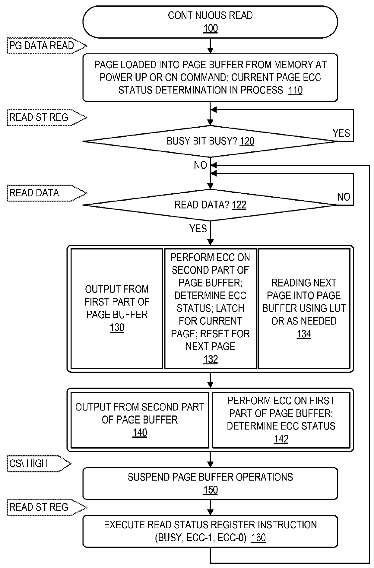
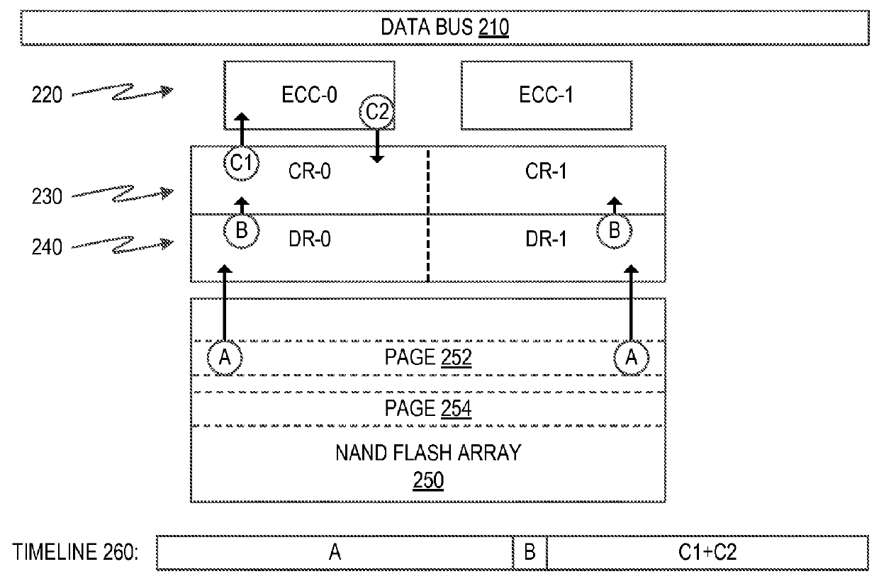
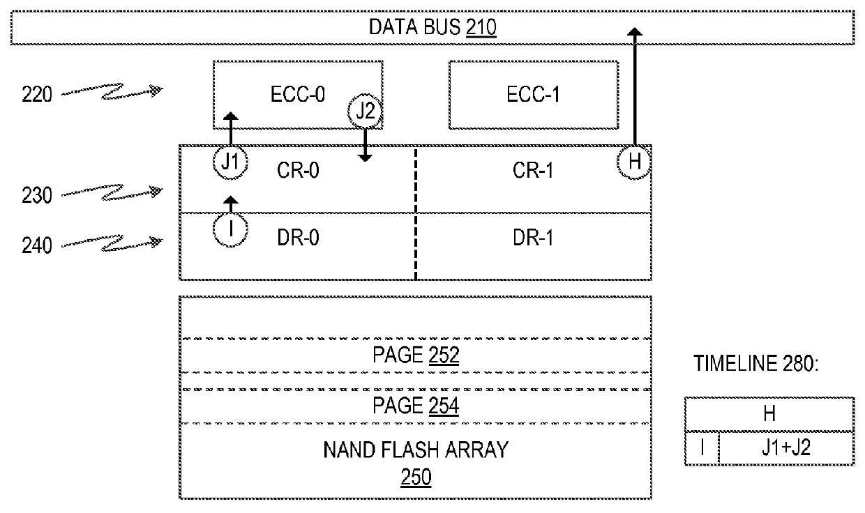
[0023]NAND memory devices may be made compatible with many characteristics of serial NOR memory devices, including: (1) the multi-I / O SPI / QPI interface; (2) small low pin count package types (as small as 8×6 mm at densities of 256 Mb and higher) such as, for example, the 8-contact WSON, 16-pin SOIC, and the 24-ball BGA type packages, with the flexibility of using larger packages such as VBGA-63 typically used with ordinary parallel and ordinary serial NAND flash memory; (3) high clock frequency operation (illustratively 104 MHz) for high transfer rates (illustratively 50 MB / Sec); (4) continuous read with Error Correction Code (“ECC”) processing across page boundaries without wait intervals, for fast code shadowing applications; (5) logically contiguous addressable good memory through bad block management which is transparent to the external systems and which is without adverse impact on the speed and continuity of the output; and (6) an output starting address of zero or alternative...


PUM


Abstract

A continuous read operation may be achieved by using a data buffer having a partitioned data register and a partitioned cache register, user configurable internal ECC associated with the cache register, and fast bad block management. During a data read operation, the ECC status may be indicated by ECC status bits. The status (1:1), for example, may indicate for the Continuous Read Mode that the entire data output contains more than 4 bits errors/page in multiple pages. However, one may wish to know the ECC status of each page or of each page partition. For the former, the ECC status for the entire page may be determined and made in the status register at the end of the output of the page. For the latter, the ECC status of each page partition may be determined and output before output of the corresponding page partition.

Description

BACKGROUND OF THE INVENTION[0001]1. Field of the Invention[0002]The present invention relates to digital memory devices and operation thereof, and more particularly to NAND flash memory having internal ECC processing and methods of operation thereof.[0003]2. Description of Related Art[0004]NAND flash memory is popular for data storage. The cost versus density advantage of single level cell (“SLC”) NAND flash memory in densities of 512 Megabits and higher is largely due to the inherently smaller memory cell size used in SLC NAND flash technology.[0005]NAND flash memory is also becoming popular for a variety of applications in addition to data storage, including code shadowing. Although commonly used SLC NAND flash memory has architectural, performance, data integrity, and bad block limitations that make it difficult to support the high speed code shadow applications for which serial NOR flash memory is well suited, various techniques have been developed to adapt NAND flash memory to ...

Claims


Application Information

Patent Timeline
Patent Type & Authority Applications(United States)
IPC IPC(8): G06F11/10G11C29/52H03M13/29
CPCG06F11/1068H03M13/29G11C29/52G11C16/26G11C2029/0411H03M13/13H03M13/1515H03M13/152H03M13/19H03M13/27
Inventor MICHAEL, ORON
Owner WINBOND ELECTRONICS CORP
Why Eureka
Try Eureka