

Bonding body, power module substrate, and heat-sink-attached power module substrate
a technology of power module and substrate, which is applied in the direction of non-electric welding apparatus, metallic pattern materials, solid-state devices, etc., can solve the problem that the heat sink cannot be bonded by the solder material, and achieve good bonding reliability
- Summary
- Abstract
- Description
- Claims
- Application Information
AI Technical Summary
Benefits of technology
Problems solved by technology
Method used
Image

Examples
first embodiment
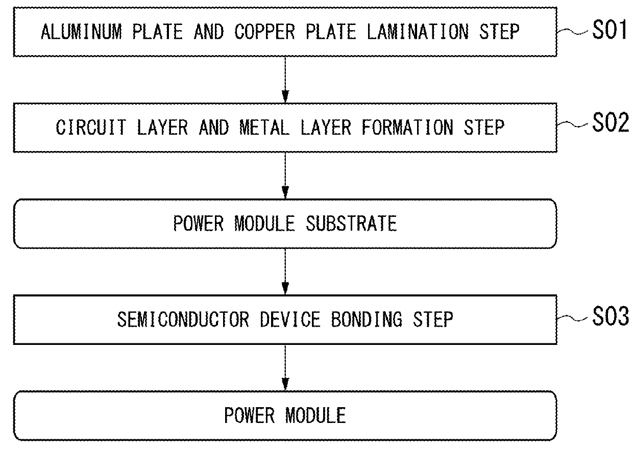
[0073]Embodiments of the present invention will be explained below with reference to the accompanying drawings. First, a first embodiment of the present invention is explained
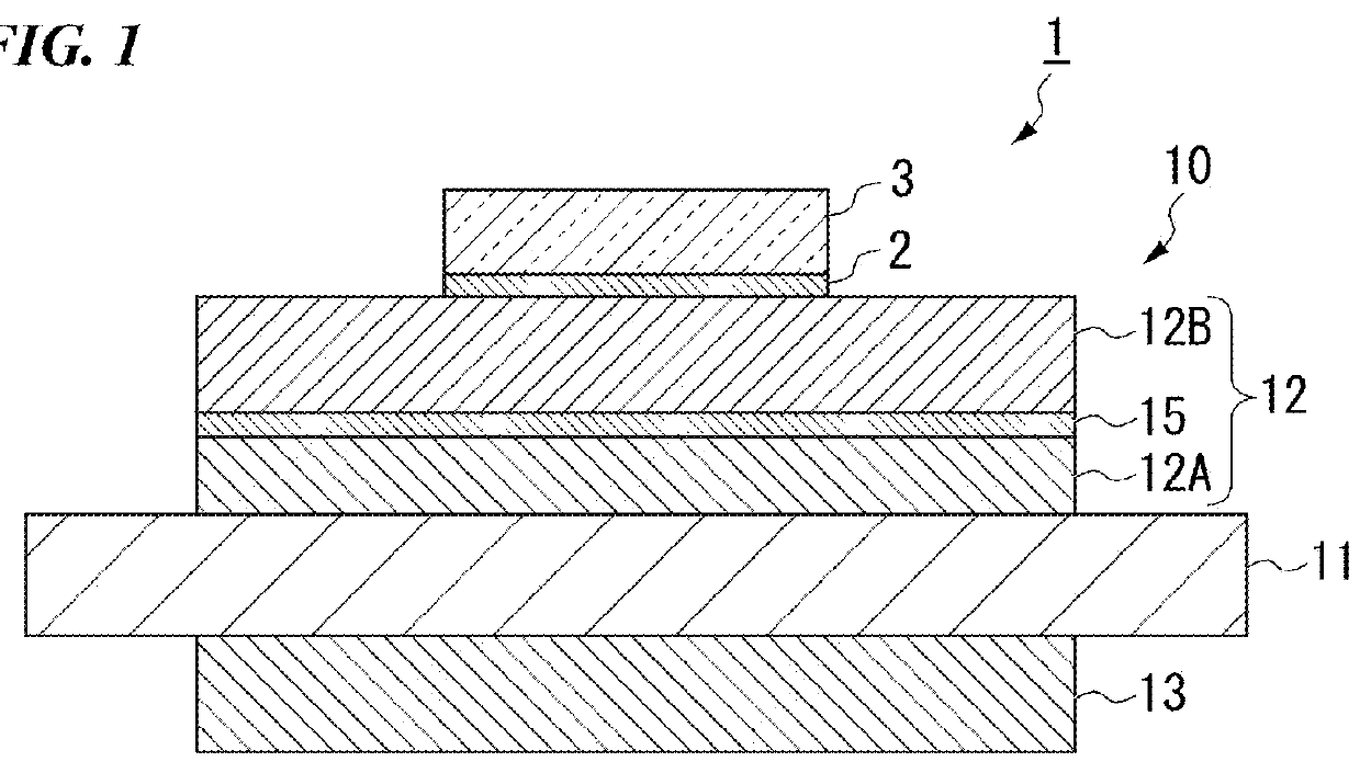
[0074]A power module 1 according to the first embodiment of the present invention is shown in FIG. 1.
[0075]The power module 1 includes the power module substrate 10 and a semiconductor device 3 bonded to one surface (upper surface in FIG. 1) of the power module substrate 10 with a solder layer 2 interposed therebetween.
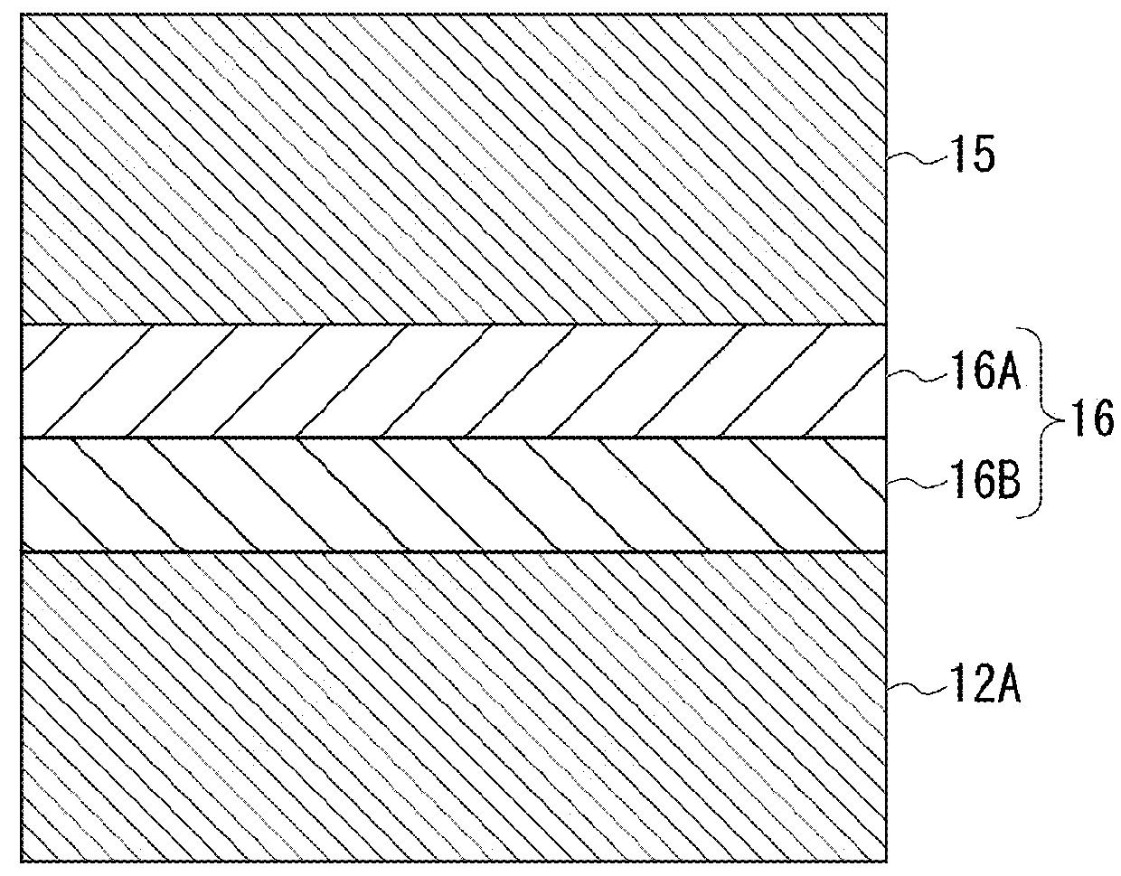
[0076]The power module substrate 10 includes; a ceramic substrate 11 constituting an insulation layer, a circuit layer 12 (bonding body) arranged on one surface (upper surface in FIG. 1 and first surface) of the ceramic substrate 11, and a metal layer 13 arranged on the other surface (second surface) of the ceramic substrate 11.
[0077]The ceramic substrate 11 is composed of AlN (aluminum nitride), Si3N4 (silicon nitride), Al2O3 (alumina), or the like, each of which has high insulation properties. ...
second embodiment
[0110]Next, a second embodiment of the present invention will be explained. In addition, with respect to the same configurations as the first embodiment, the same reference numerals are used and the detail explanations thereof are omitted.
[0111]A heat-sink-attached-power module 201 according to the second embodiment of the present invention is shown in FIG. 5. The heat-sink-attached-power module 201 includes a heat-sink-attached-power module substrate 230, and a semiconductor device 3 bonded to one surface (upper surface in FIG. 5) of the heat-sink-attached-power module substrate 230 with a solder layer 2 interposed therebetween. The heat-sink-attached-power module substrate 230 includes a power module substrate 210, and a heat sink 231 (metal member) laminated to a lower side of the power module substrate 210 with a Ti layer 215 interposed therebetween.
[0112]As shown in FIG. 5, the power module substrate 210 includes: a ceramic substrate 11, a circuit layer 212 arranged on a first ...
fifth embodiment
[0137]A heat-sink-attached-power module 501 according to the fifth embodiment of the present invention is shown in FIG. 13.
[0138]The heat-sink-attached-power module 501 includes a heat-sink-attached-power module substrate 530, and a semiconductor device 3 bonded to one surface (upper surface in FIG. 13) of the heat-sink-attached-power module substrate 530 with a solder layer 2 interposed therebetween.
[0139]The heat-sink-attached-power module substrate 530 includes a power module substrate 510, and a heat sink 531 bonded to a lower side of the power module substrate 510 with a solder layer 535 interposed therebetween.
[0140]As shown in FIG. 14, the power module substrate 510 includes; a ceramic substrate 511 constituting an insulation layer, a circuit layer 512 arranged on one surface (upper surface in FIG. 14 and first surface) of the ceramic substrate 511, and a metal layer 513 arranged on the other surface (lower surface in FIG. 15 and second surface) of the ceramic substrate 511.
[...
PUM
| Property | Measurement | Unit |
|---|---|---|
| thickness | aaaaa | aaaaa |
| thickness | aaaaa | aaaaa |
| thickness | aaaaa | aaaaa |
Abstract
Description
Claims
Application Information