Integrated photonic component and method of designing the same
- Summary
- Abstract
- Description
- Claims
- Application Information
AI Technical Summary
Benefits of technology
Problems solved by technology
Method used
Image

Examples
Embodiment Construction
[0084]The abovementioned and other features and effects of the present invention will be explained in more detail below with reference to the abovementioned drawings in which preferred and illustrative embodiments of the invention are shown. The skilled person will realize that other alternatives and equivalent embodiments of the invention can be conceived and reduced to practice without departing from the scope of the present invention.
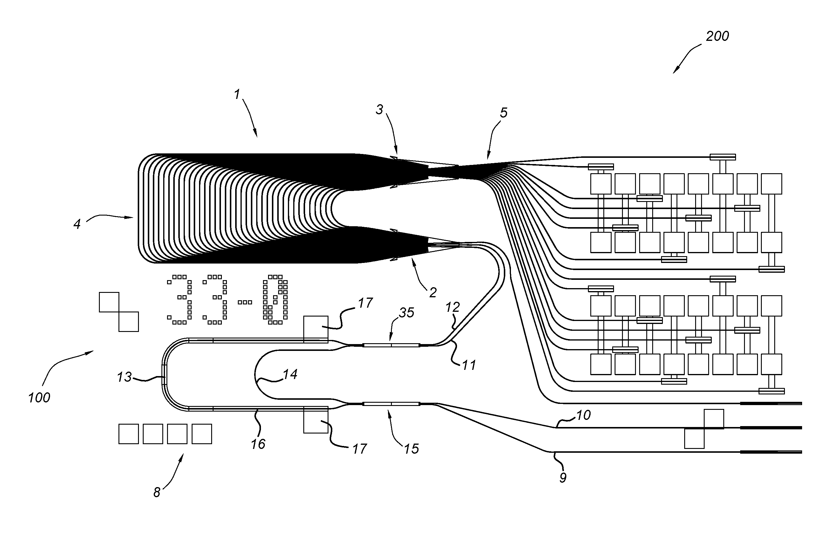
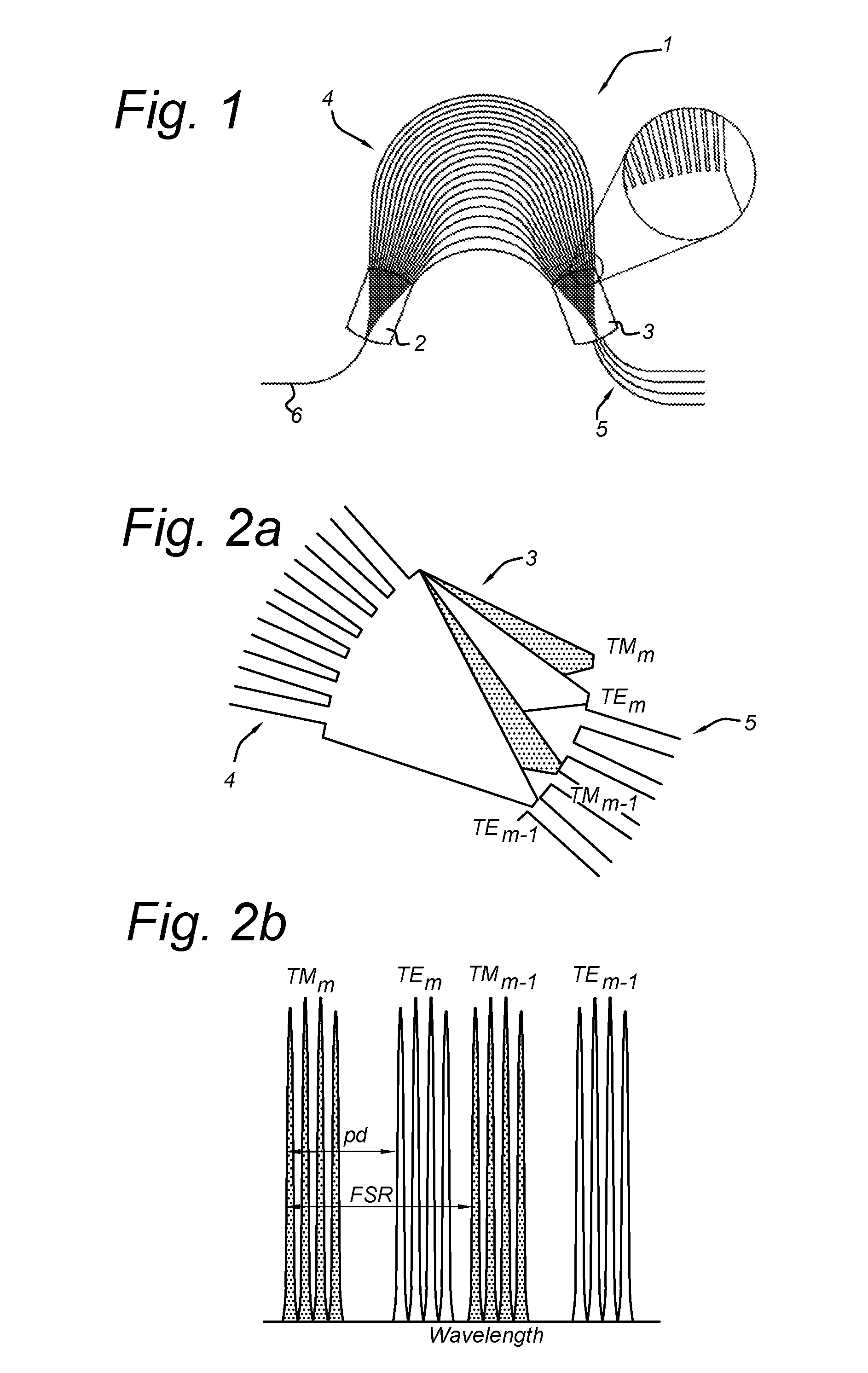
[0085]FIGS. 1, 2a and 2b have been discussed in the introduction reciting the background of the invention.
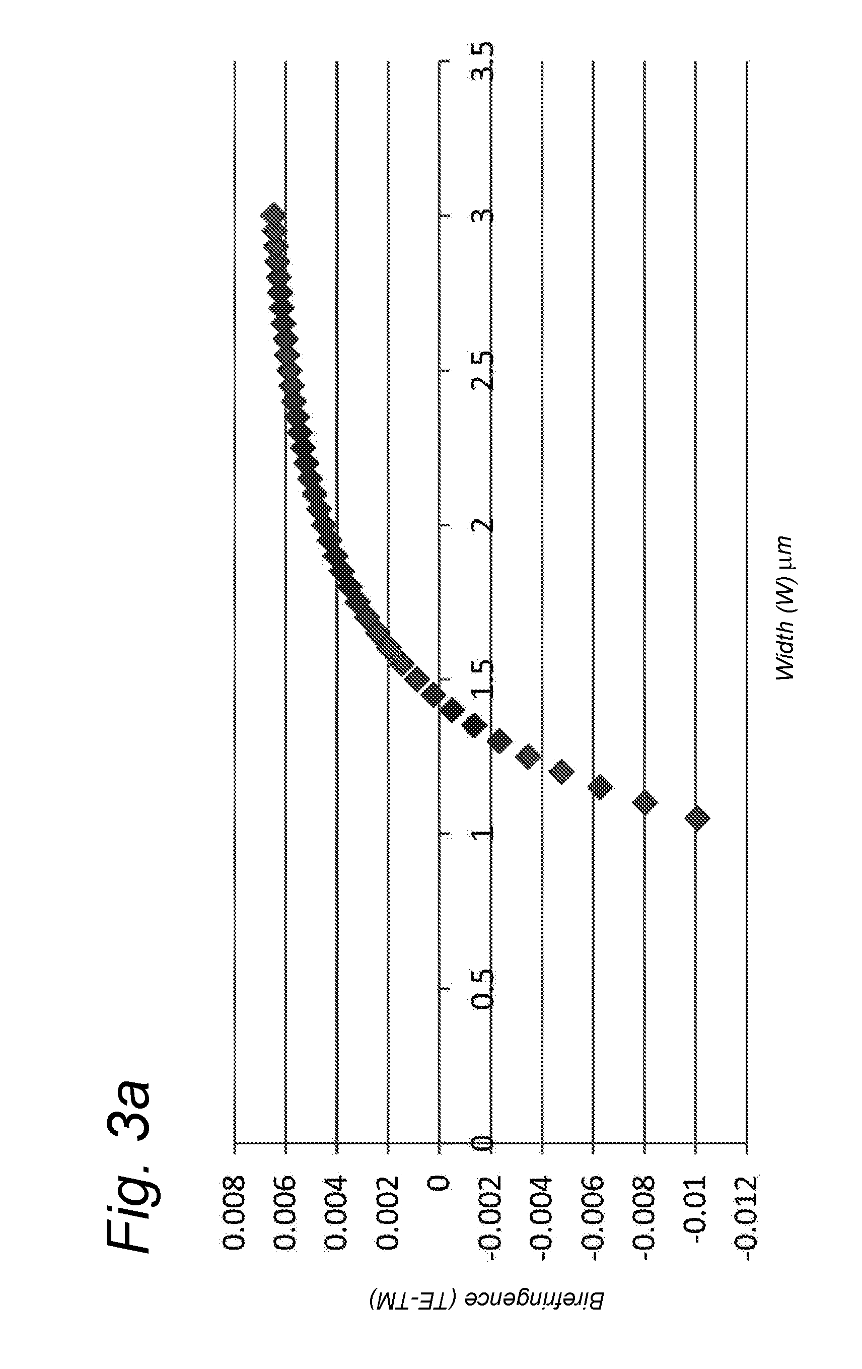
[0086]In standard InP waveguides the difference between the mode indices for TE and TM polarizations (ΔNeff,TE-TM), also called the birefringence, depends on the waveguide width (W). FIG. 3a schematically shows typical waveguide birefringence for InP waveguides as a function of waveguide width (W) in micrometer. There is a certain waveguide width (around W=1.45 μm) for which the birefringence (ΔNeff,TE-TM) is zero, but a sm...
PUM
 Abstract
Description
Claims
Application Information
 - R&D
- Intellectual Property
- Life Sciences
- Materials
- Tech Scout
- Unparalleled Data Quality
- Higher Quality Content
- 60% Fewer Hallucinations
Browse by: Latest US Patents, China's latest patents, Technical Efficacy Thesaurus, Application Domain, Technology Topic, Popular Technical Reports.
© 2025 PatSnap. All rights reserved.Legal|Privacy policy|Modern Slavery Act Transparency Statement|Sitemap|About US| Contact US: help@patsnap.com