Vsl-based vt-compensation and analog program scheme for NAND array without csl

Active Publication Date: 2016-02-18
APLUS FLASH TECH
View PDF1 Cites 69 Cited by
  • Summary
  • Abstract
  • Description
  • Claims
  • Application Information

AI Technical Summary

Benefits of technology

[0052]In yet another embodiment, the present invention further discloses that the SLC-WL cells are configured to quickly store PB data from external off-chip DRAM CACHE registers when power supply of Vdd is suddenly removed. For this mixed TLC+SLC NAND array, a batch-base concurrent SLC program and program-verify on multiple selected SLC WLs can be performed to reduce the latency. The M pages off-chip DRAM N-bit digital data can be sequentially loaded in M corresponding N-bit PCACHE registers in M dispersed LGs distributed among multiple MGs and HGs of the mixed TLC+SLC NAND array first and then performed an ABL multi-page concurrent N-bit SLC program on M selected SLC WLs in M 4-WL units without increasing the PB sizes in peripheral area to reduce the die sizes and program speed and need of a costly super-large Vdd capacitors to store the Vdd voltage for preparing a sudden power down. After Vdd being powered up again, the M pages of stored SLC data in M SLC-WLs in M 4-WL units can be concurrently programmed into the desired TLC in background program. In one or more embodiments, multiple SLC WL cells can be performed multiple TLC WLs on the same time to reduce the latency and power consumption.
[0053]In following description, when N-bit is referred, it means that total 16 KB physical NAND cells in 16 KB LBL lines residing in one physical WL or page not including the additional syndrome ECC bytes. In this application, N-bit means a full physical WL page of 16 KB cells. Thereby, N/2-bit means 8 KB which is ½ of one full physical page or ½ WL size storing 8 KB regular NAND cells. 16 KB and N-bit or 8 KB and N/2-bit are alternately used in this description and should be treated as the same. As explained later, each short LBL line is associa

Problems solved by technology

Unfortunately, a typical NAND array is usually formed in a very compact memory matrix to squeeze die size smaller.
When NAND technology scaling comes to below 30 nm, or even down to 10 nm-class range, the floating-gate Vt interfering coupling effect becomes very severe between adjacent BLs and WLs.
The Yupin coupling effect will result in the nLC data reliability issue of unintentional error-bit reading, which is undesired but in fact not avoidable.
However, this is not a perfect BL-shielding method as the BL-BL coupling effect still happens, causing penalties of 2-fold latency of read and program-verify operation, 2-fold Vpass and Vread WL gate disturbance to degrade P/E endurance cycle data reliability of NAND products, and 2-fold power consumption of read, program and verify due to 2 times of half-page size access operations.
On the other hand, although the ABL me

Method used


Image

  • Vsl-based vt-compensation and analog program scheme for NAND array without csl
  • Vsl-based vt-compensation and analog program scheme for NAND array without csl
  • Vsl-based vt-compensation and analog program scheme for NAND array without csl

Examples


Embodiment Construction

[0161]In the following detailed description of the present embodiments, reference is made to the accompanying drawings that forms a part hereof, and in which is shown, by way of illustration, specific embodiments in which the disclosure may be practiced. In the drawings, like numerals describe substantially similar components throughout the several views. These embodiments are described in sufficient detail to enable those skilled in the art to practice the embodiments. Other embodiments may be utilized and structural, logical, and electrical changes may be made without departing from the scope of the present disclosure. The following detailed description, therefore, not to be taken in a limitation sense.

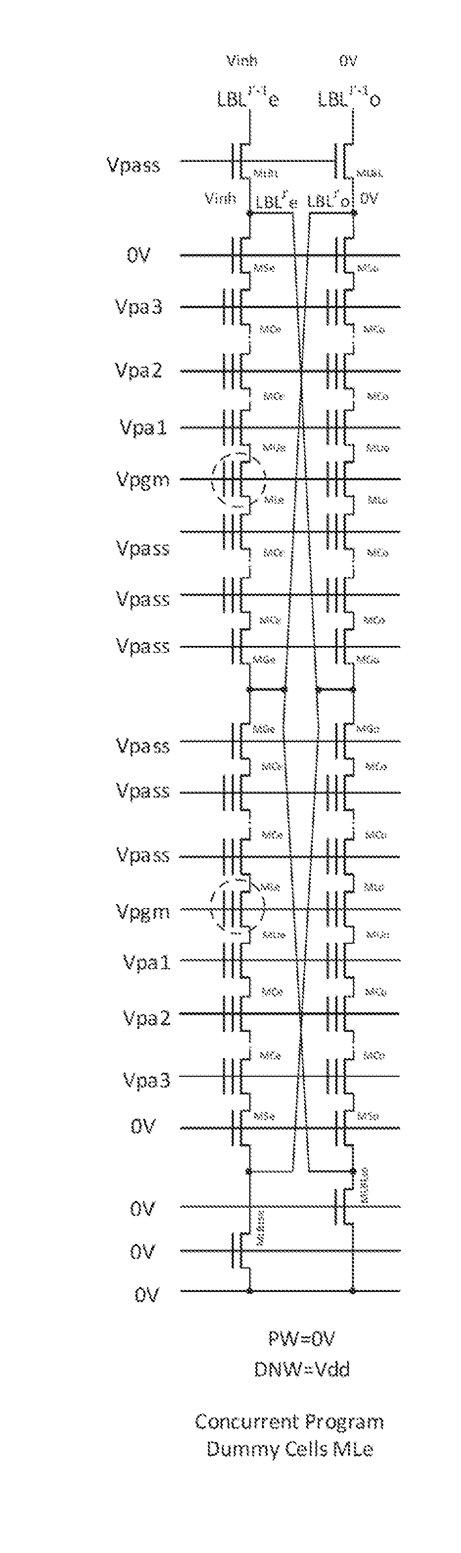
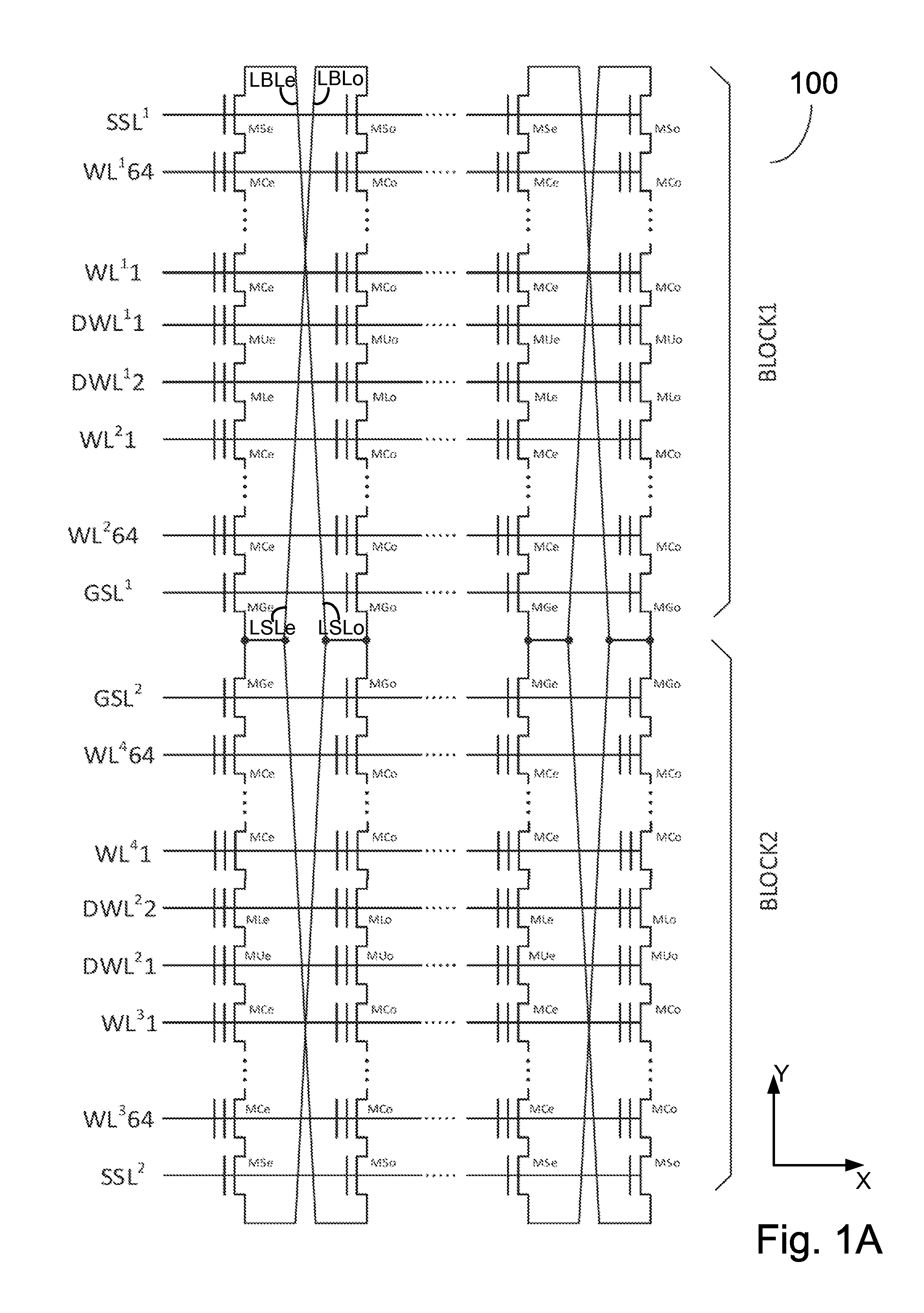
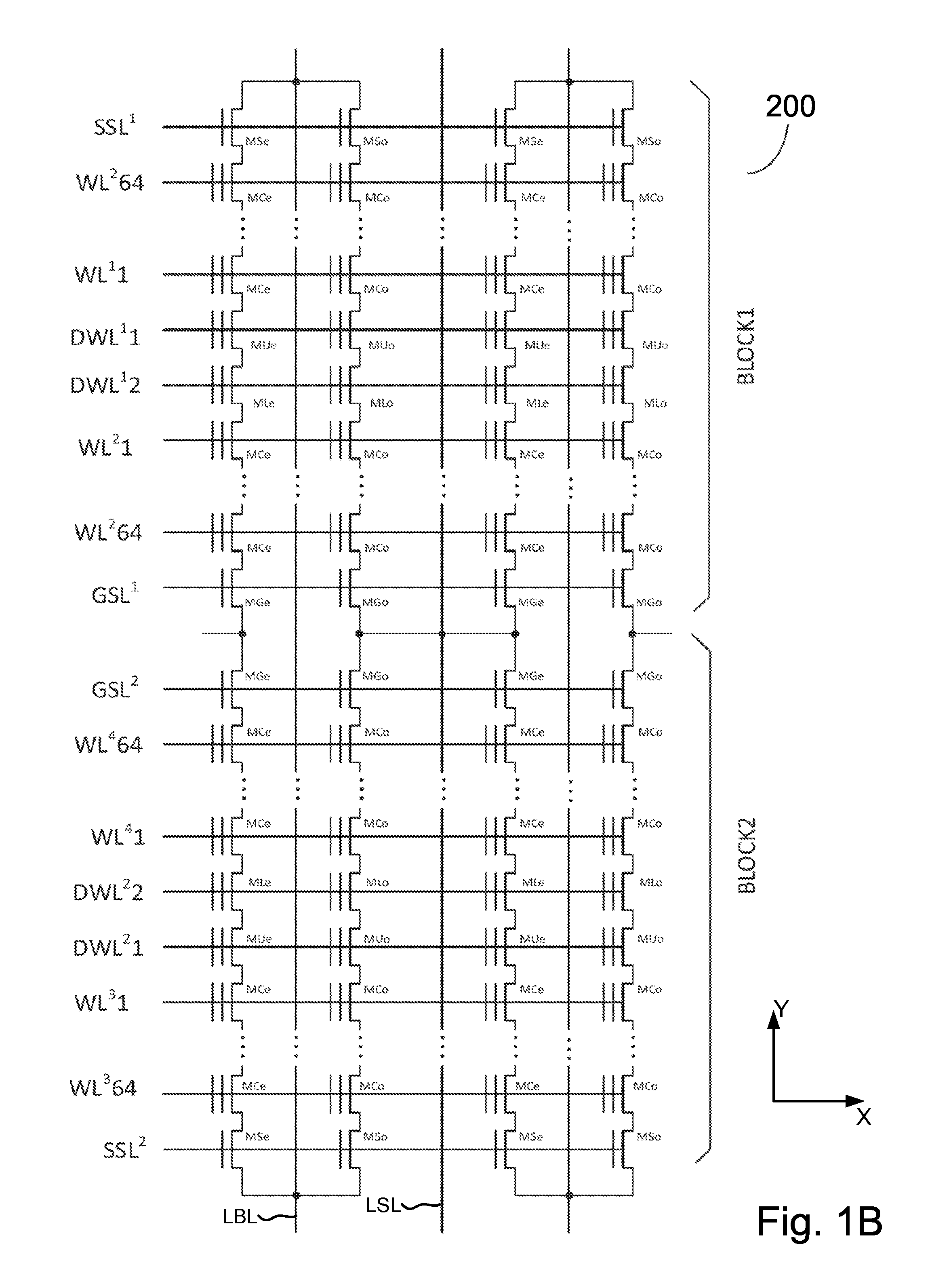
[0162]So far, almost of all 2D non-hierarchical NAND key operations are performed in unit of single WL in one selected NAND plane. Although there are many prior art disclosing operation on multiple WLs in multiple independent blocks in multiple independently different planes, there ...


PUM


Abstract

A YUKAI NAND array comprising multiple strings of all TLC and mixed TLC+SLC memory cells associated with hierarchical global/local bit lines (GBL/LBL) and each string being associated with one LBL and having adjacent LBL as a dedicated local source line (LSL) with full BL-shielding without wasting extra silicon area and without a common source line to connect all strings. Each of the LBLs is interleavingly associated with either an Odd or Even string selected via one pair of dummy cells inserted in each string and is used as one on-chip PCACHE register with full BL-shielding to perform concurrent ABL, AnP and Alt-WL program under multi-passes program schemes with LBL program voltage compensations and half-BL Odd/Even program-verify and read operations with individual VSL-based Vt-compensation to mitigate high WL-WL and BL-BL coupling effects.

Description

1. CROSS-REFERENCES TO RELATED APPLICATIONS[0001]This application claims priority to U.S. Provisional Application No. 62 / 038,329 entitled “VSL-BASED Vt-COMPENSATION FOR MIXED TLC+SLC NAND”, filed Aug. 17, 2014, commonly assigned and incorporated by reference herein for all purposes.[0002]This application is related to U.S. patent application Ser. Nos. 14 / 806,629, 14 / 583,178, 14 / 487,078, 14 / 341,739, 14 / 316,936, and 14 / 283,209, incorporated by reference herein for all purposes.[0003]This application is related to following U.S. Pat. Nos. 5,867,429; 6,542,407; 6,522,580; 6,781,877; 6,807,095; 6,847,553; 6,870,768; 6,888,758; 6,917,542; 7,046,548; 7,061,798; 7,102,924; 7,187,585; 7,196,928; 7,196,946; 7,196,928; 7,224,613; 7,289,344; 7,289,348; 7,301,808; 7,301,813; 7,301,839; 7,315,477; 7,321,510; 7,372,730; 7,397,698; 7,443,729; 7,499,329; 7,506,113; 7,522,454; 7,652,929; 7,876,611; 7,876,611; 8,036,041; 8,130,556; 8,274,823; 8,284,606; 8,284,613; 8,400,839; 8,570,810; 8,638,608; 8,70...

Claims


Application Information

Patent Timeline
IPC IPC(8): G11C11/56G11C16/04G11C16/10G11C16/26G11C16/34
CPCG11C11/5635G11C11/5642G11C11/5671G11C16/3459G11C16/26G11C16/0483G11C16/10G11C7/18G11C16/08G11C16/3427G11C2207/2245G11C2211/5641
Inventor LEE, PETER, WUNG
Owner APLUS FLASH TECH
Why Eureka
Try Eureka