
Integrated CMOS/MEMS Microphone Die Components

a technology of cmos/mems and microphone die, applied in the field of microelectronics, can solve the problems of leaving the bonding pads on the top surface unaffected, and achieve the effects of reducing the weight of the device, preventing further upward and preventing further downward movement of the diaphragm

Active Publication Date: 2016-03-03
KNOWLES ELECTRONICS INC
View PDF4 Cites 6 Cited by
  • Summary
  • Abstract
  • Description
  • Claims
  • Application Information

AI Technical Summary

Benefits of technology

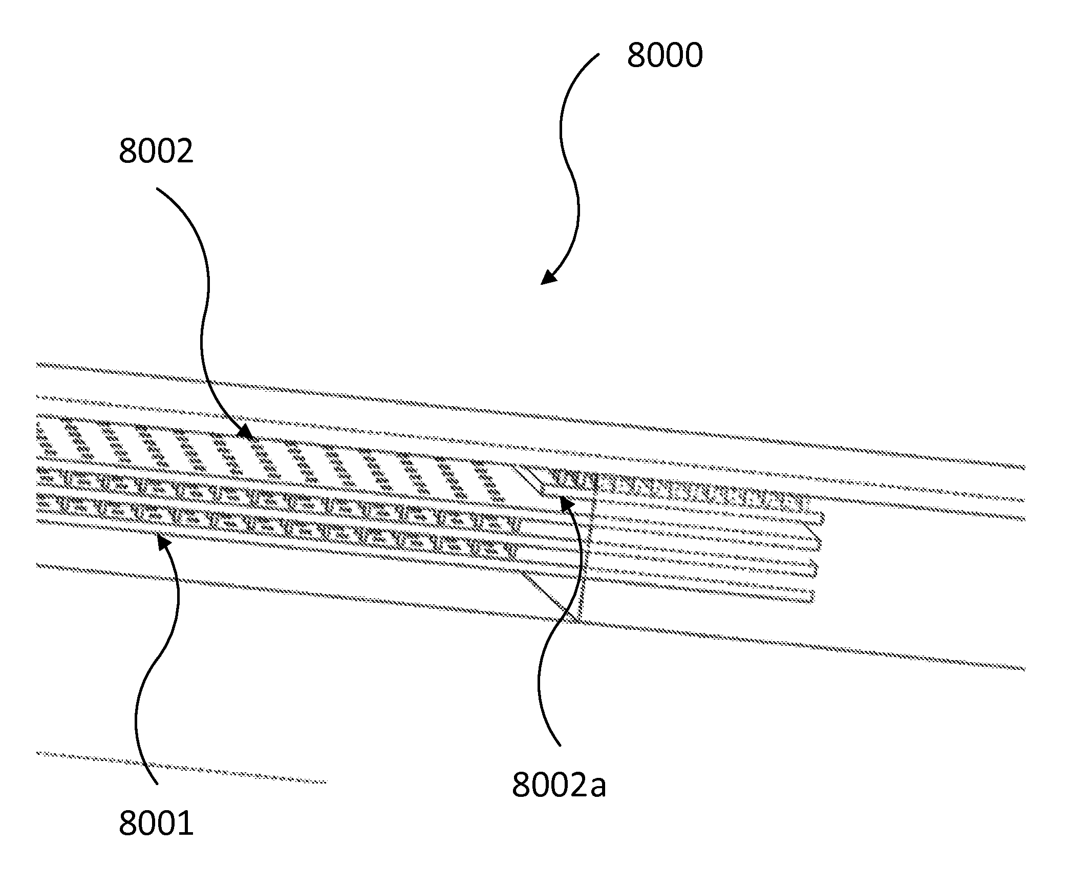
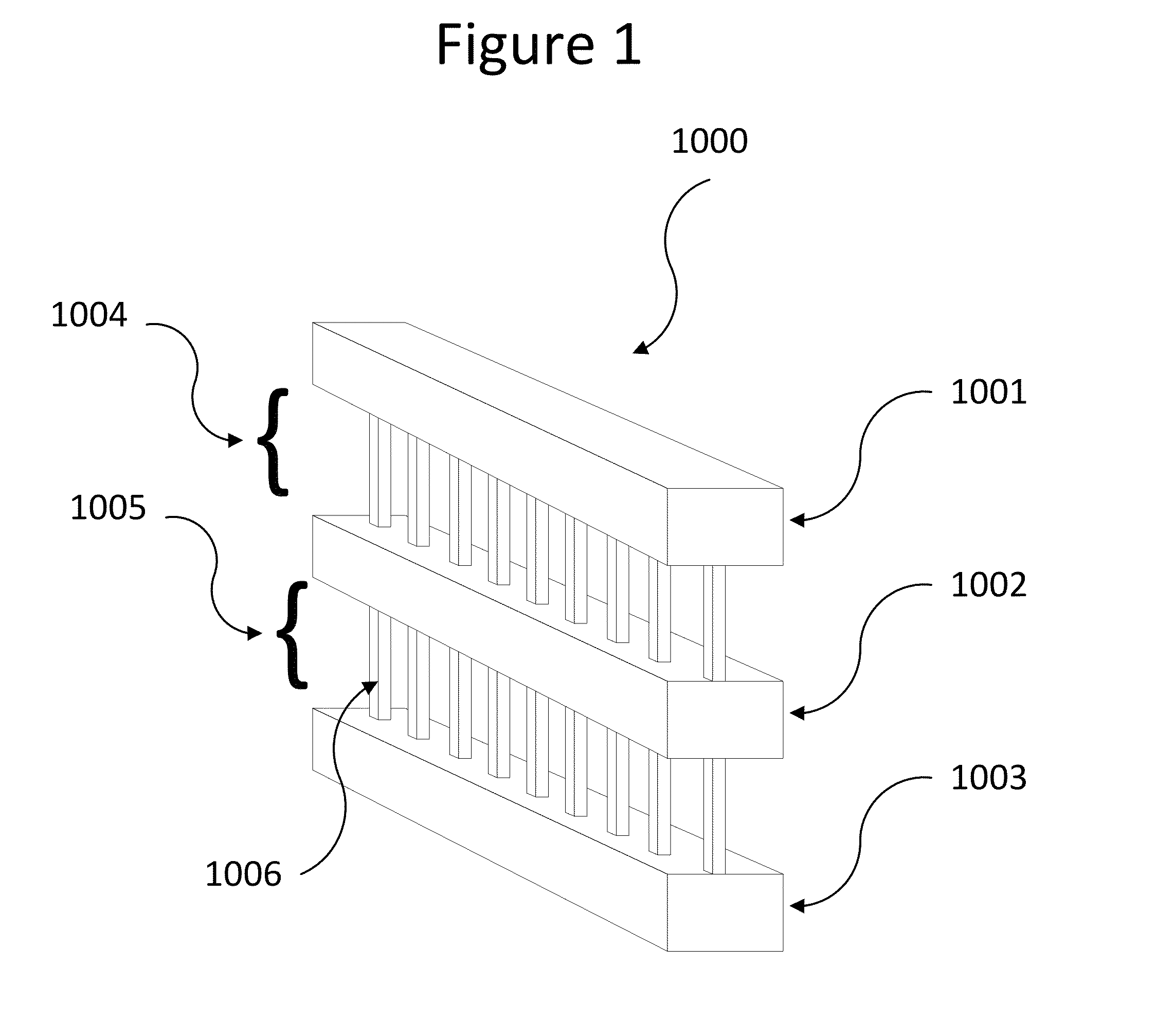
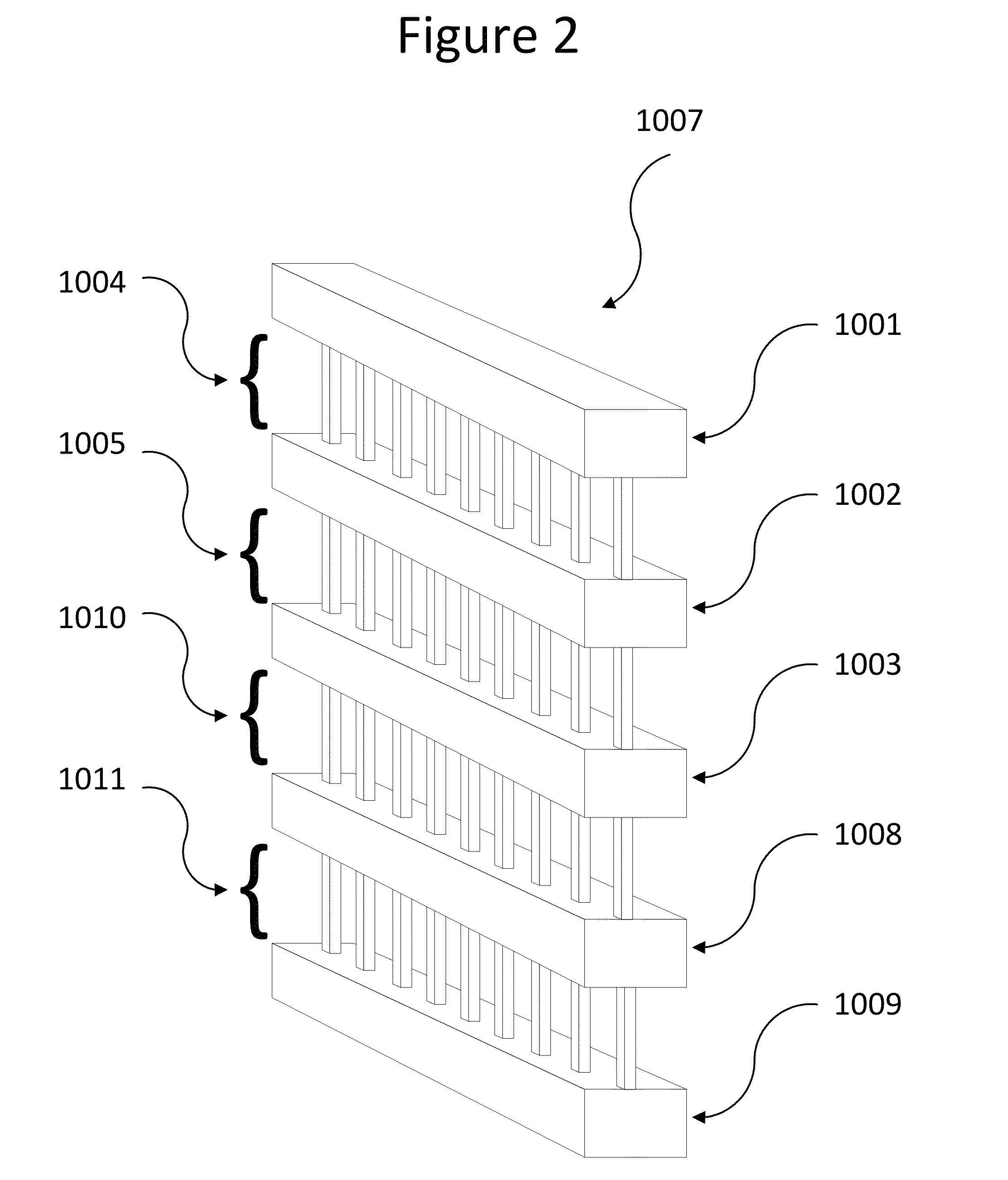
The patent describes a method for making a microphone with a movable diaphragm. The method involves etching a cavity in the diaphragm and adding a layer of metal on the bottom of the diaphragm to provide stability during operation. A plate made of multiple layers of metal and dielectric material is used to create the diaphragm, with metal vias between the layers. The etchant can be introduced through a hole in the bottom of the wafer, which is simpler and cheaper than adding a patterned cap wafer to the top of the wafer. The patent also describes how the use of multiple alternating layers of metal and dielectric material can be used to create a more efficient and lightweight microphone. The invention also mentions the use of selective etching and the removal of certain metallic layers to limit movement and reduce weight.

Problems solved by technology

Further, sealing the bottom of the wafer leaves the bonding pads on the top surface unaffected.

Method used


Image

  • Integrated CMOS/MEMS Microphone Die Components
  • Integrated CMOS/MEMS Microphone Die Components
  • Integrated CMOS/MEMS Microphone Die Components

Examples


Embodiment Construction

[0041]The following sections set forth numerous specific embodiments taking advantage of various aspects of the invention. These are not intended to be an exhaustive collection of every embodiment of the invention, as embodiments of the invention can be combined in a multiplicity of ways without departing from the principles of the invention.

General Fabrication Techniques

[0042]The embodiments disclosed can be fabricated using standard sub-micron CMOS fabrication techniques known to one of skill in the art, for example:

[0043]1. On the portions of a silicon wafer substrate intended to be populated by transistors, build the transistors using standard CMOS techniques. The portions of the wafer for the MEMS structures remain untouched, leaving the field oxide in this area.

[0044]2. Deposit a layer of SiO2 over the entire wafer.

[0045]3. Apply a patterned mask onto the SiO2 layer with openings for the electrical vias needed for the transistor interconnects and for the vias needed for the st...


PUM


Abstract

The claim invention is directed at a MEMS microphone die fabricated using CMOS-based technologies. In particular, the claims are directed at various aspects of a diaphragm for a MEMS microphone die which is fabricated as stacked metallic layers separated by vias using CMOS fabrication technologies.

Description

RELATED APPLICATIONS[0001]This application claims the benefit of U.S. Provisional Patent Application 61 / 871,957, filed on Aug. 30, 2013, and Patent Cooperation Treaty Application PCT / US14 / 53235, filed on Aug. 28, 2014. These applications are hereby incorporated by reference in their entireties for all purposes.BACKGROUND OF THE INVENTION[0002]In the 1960s, practitioners in the field of microelectronics first developed techniques for fabricating tiny mechanical structures using a series of steps involving the depositing of layers of materials onto the surface of a silicon wafer substrate, followed by selectively etching away parts of the deposited materials. By the 1980s, the industry began moving toward silicon-based surface micromachining using polysilicon as the mechanical layer. However, although polysilicon has proven a useful building block in fabricating microelectromechanical systems (MEMS) because of its mechanical, electrical, and thermal properties, fabrication techniques ...

Claims


Application Information

Patent Timeline
IPC IPC(8): B81B7/00H04R7/10H04R19/00H04R19/04H04R31/00
CPCB81B7/007H04R19/04H04R19/005H04R7/10H04R2307/027B81B2203/0127B81B2201/0257H04R2201/003H04R31/003B81B3/0051B81B3/007B81C2203/0145B81C2203/0714
Inventor LOEPPERT, PETER, V.
Owner KNOWLES ELECTRONICS INC
Learn More