Fin field-effect transistors and fabrication methods thereof

a field-effect transistor and transistor technology, applied in the direction of transistors, semiconductor devices, electrical equipment, etc., can solve the problems of inability to match existing methods to desired requirements, difficulty in pinching off the channel regions of semiconductor devices, and worse control ability of gate structures of semiconductor devices to the channel regions

Active Publication Date: 2016-03-03
SEMICON MFG INT (SHANGHAI) CORP
View PDF5 Cites 24 Cited by
  • Summary
  • Abstract
  • Description
  • Claims
  • Application Information

AI Technical Summary

Problems solved by technology

Thus, the control ability of the gate structures of the semiconductor devices to the channel regions become worse.
That is, the pinch off of the channel regions of the semiconductor devices has become more and more difficult.
However, the quality of embedded SiGe structures, are also referred as a stress layer, i.e., material layers applying the compressive stress or tensile stress to the channel regions of the FinFETs, formed by existing methods may not match desired requirements.
Thus, the electrical properties of the FinFETs having such a stress layer may not match requirements neither.

Method used


Image

  • Fin field-effect transistors and fabrication methods thereof
  • Fin field-effect transistors and fabrication methods thereof
  • Fin field-effect transistors and fabrication methods thereof

Examples


Embodiment Construction

[0015]Reference will now be made in detail to exemplary embodiments of the invention, which are illustrated in the accompanying drawings. Wherever possible, the same reference numbers will be used throughout the drawings to refer to the same or like parts.

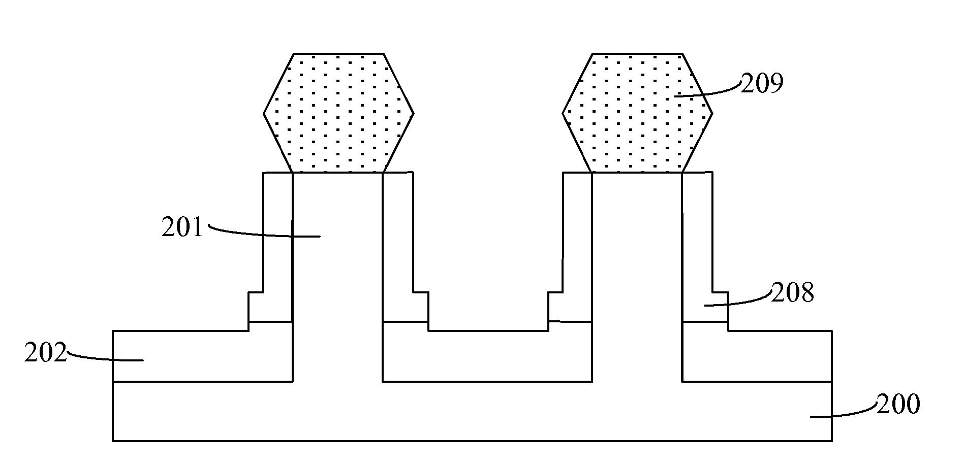
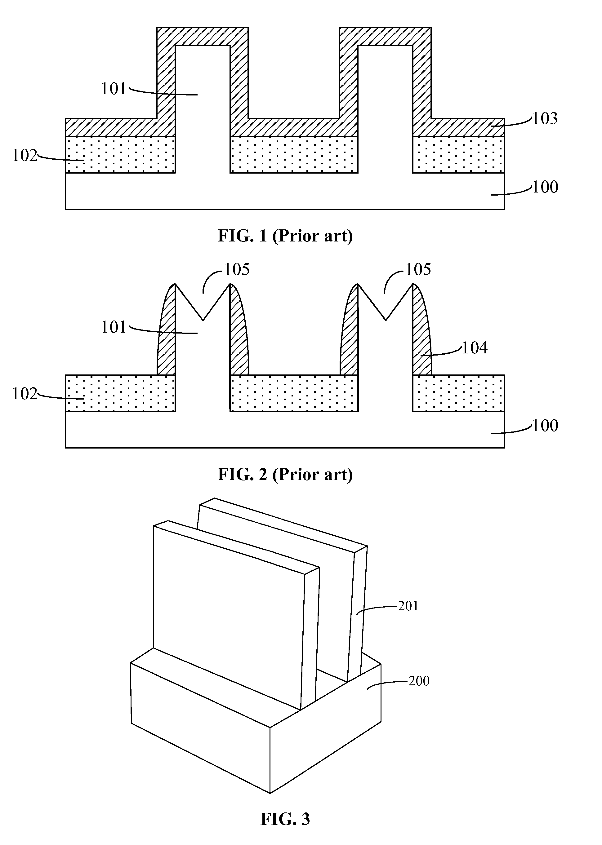
[0016]FIGS. 1-2 illustrate semiconductor structures corresponding to certain stages of an existing fabrication process of FinFETs. As shown in FIG. 1, the process includes providing substrate 100; forming a plurality of fins 101 on the substrate 100; and forming an insulation layer 102 on the substrate 100 between adjacent fins 101. The insulation layer 102 covers portions of the side surfaces of the fins 101. Further, the surface of the insulation layer 102 is lower than the top surfaces of the fins 101. The process also includes forming a barrier layer 103 covering the surface of the insulation layer 102, and the top and the side surfaces of the fins 101.

[0017]Further, as shown in FIG. 2, the process includes removing the portion...


PUM


Abstract

A method for forming FinFETs includes, sequentially, providing a substrate; forming a plurality of fins on a surface of the substrate; forming a gate structure overlying on at least one of the plurality of fins; forming a barrier layer covering top and side surfaces of the gate structures, and top and side surfaces of the plurality of fins; performing a radical oxidation process to convert a top portion of the barrier layer to a passive layer to form a remaining barrier layer and to cause the top surfaces of the fins to be flat after subsequent etching processes; performing an etch-back process on the passive layer to form passive sidewalls on side surfaces of the portions of the remaining barrier on the side surfaces of the fins; and removing portions of the remaining barrier layer on the top surfaces of the fins by a wet etching process using the passive sidewalls as an etching mask.

Description

CROSS-REFERENCES TO RELATED APPLICATIONS[0001]This application claims the priority of Chinese patent application No. 201410445807.6, filed on Sep. 3, 2014, the entirety of which is incorporated herein by reference.FIELD OF THE INVENTION[0002]The present invention generally relates to the field of semiconductor manufacturing technology and, more particularly, relates to Fin field-effect transistors (FinFETs) and fabrication processes thereof.BACKGROUND[0003]With the continuous development of the semiconductor technology, the technical node of the semiconductor processes has become smaller and smaller by following the Moore's law. In order to match the requirements for decreasing the technical node, the channel length of MOSFETs has been continuously decreased. Decreasing the channel length of MOSFETs may bring some advantages, such as increasing the integration level, and increasing the switch speed of the MOSFETs, etc.[0004]However, with the decreasing of the channel length of the s...

Claims


Application Information

Patent Timeline
Patent Type & Authority Applications(United States)
IPC IPC(8): H01L27/088H01L21/02H01L21/311H01L21/8234H01L29/165H01L29/78
CPCH01L27/0886H01L21/823431H01L21/0223H01L21/31111H01L21/31144H01L21/823468H01L21/02636H01L21/0217H01L21/0214H01L21/31116H01L29/7842H01L29/165H01L21/02164H01L29/7848H01L21/02326H01L21/02337H01L21/0234H01L29/66795H01L29/785
Inventor YU, GUOBIN
Owner SEMICON MFG INT (SHANGHAI) CORP
Why Eureka
Try Eureka