Tie-off structures for middle-of-line (MOL) manufactured integrated circuits, and related methods

a technology of integrated circuits and tie-off structures, which is applied in the direction of electrical apparatus, semiconductor devices, semiconductor/solid-state device details, etc., can solve the problems of gate contact formation during the mol process, the pressure to increase processing capabilities while decreasing the size of the integrated circuit (ics), and the conventional manufacturing process is strained, so as to achieve sufficient connectivity and simplify the manufacturing of the integrated circuit (ics)

Inactive Publication Date: 2016-03-17
QUALCOMM INC
View PDF2 Cites 17 Cited by
  • Summary
  • Abstract
  • Description
  • Claims
  • Application Information

AI Technical Summary

Benefits of technology

[0007]Aspects disclosed in the detailed description include tie-off structures for middle-of-line (MOL) manufactured integrated circuits, and related methods. As a non-limiting example, the tie-off structure may be used to tie-off a drain or source of a transistor to the gate of the transistor, such as provided in a dummy gate used for isolation purposes. In this regard in one aspect, a MOL stack is provided that includes a metal gate connection and is coupled to a metal layer through a metal structure disposed in and above a dielectric layer above a gate associated with the metal gate connection. By coupling the metal gate connection to the metal layer, the gate may be coupled or “tied-off” to a source or drain element of a transistor of which the gate is an element. As an example, moving the coupling to in and above the dielectric layer of the MOL stack helps avoid the need to etch the metal gate connection provided below the dielectric layer to provide sufficient connectivity between the metal layer and the metal gate connection, thus simplifying the manufacturing of integrated circuits (ICs), particularly at low nanometer node sizes.

Problems solved by technology

The pressures to increase processing capabilities while decreasing the size of the integrated circuits (ICs) have strained conventional manufacturing processes, especially as the node size within ICs has been reduced to low nanometer (nm) dimensions (e.g., <20 nm).
In particular, gate contact formation during the MOL process is increasingly challenging at the current low nanometer node sizes, particularly for lithography printing.

Method used


Image

  • Tie-off structures for middle-of-line (MOL) manufactured integrated circuits, and related methods
  • Tie-off structures for middle-of-line (MOL) manufactured integrated circuits, and related methods
  • Tie-off structures for middle-of-line (MOL) manufactured integrated circuits, and related methods

Examples


Embodiment Construction

[0020]With reference now to the drawing figures, several exemplary aspects of the present disclosure are described. The word “exemplary” is used herein to mean “serving as an example, instance, or illustration.” Any aspect described herein as “exemplary” is not necessarily to be construed as preferred or advantageous over other aspects.

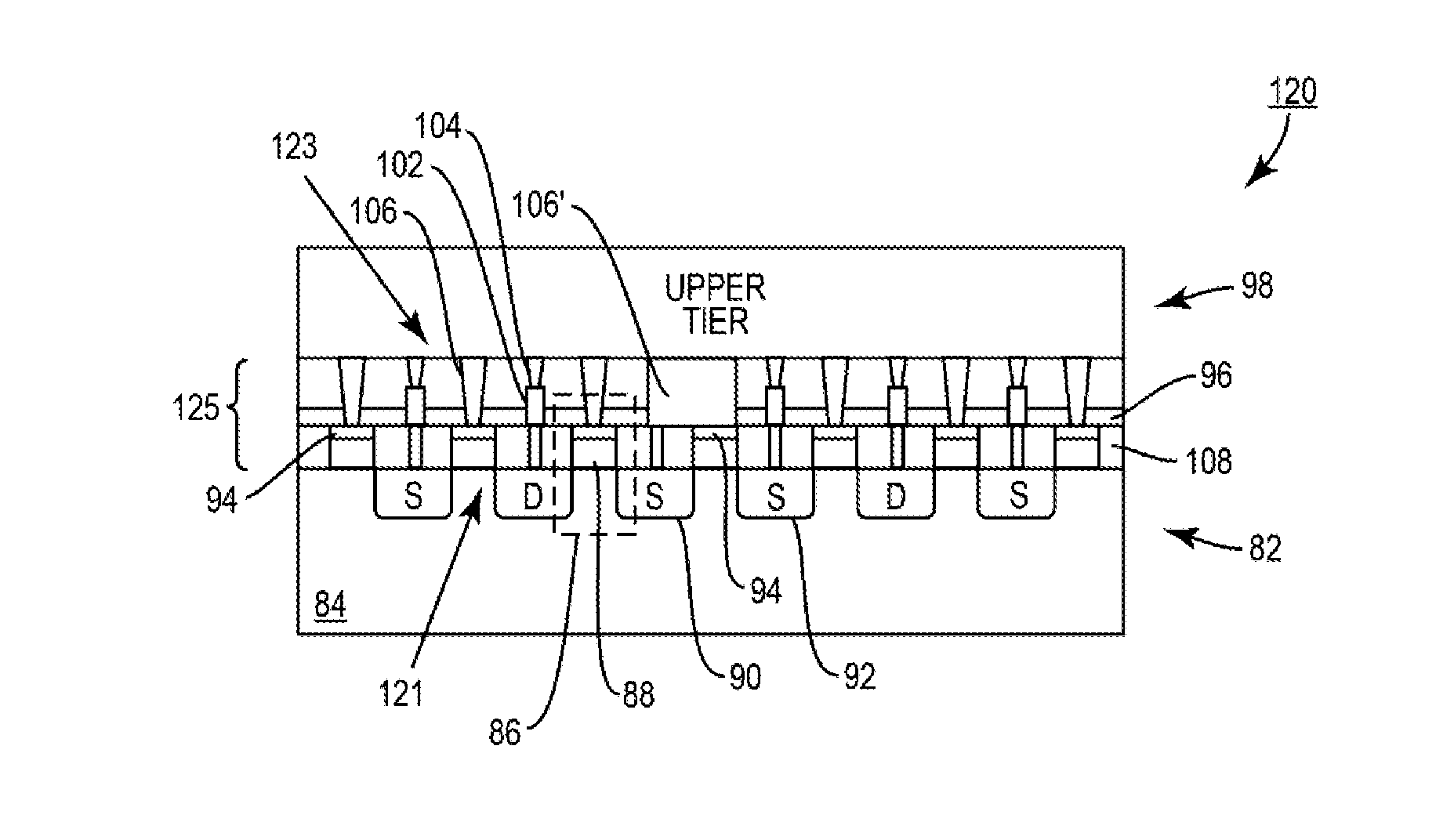
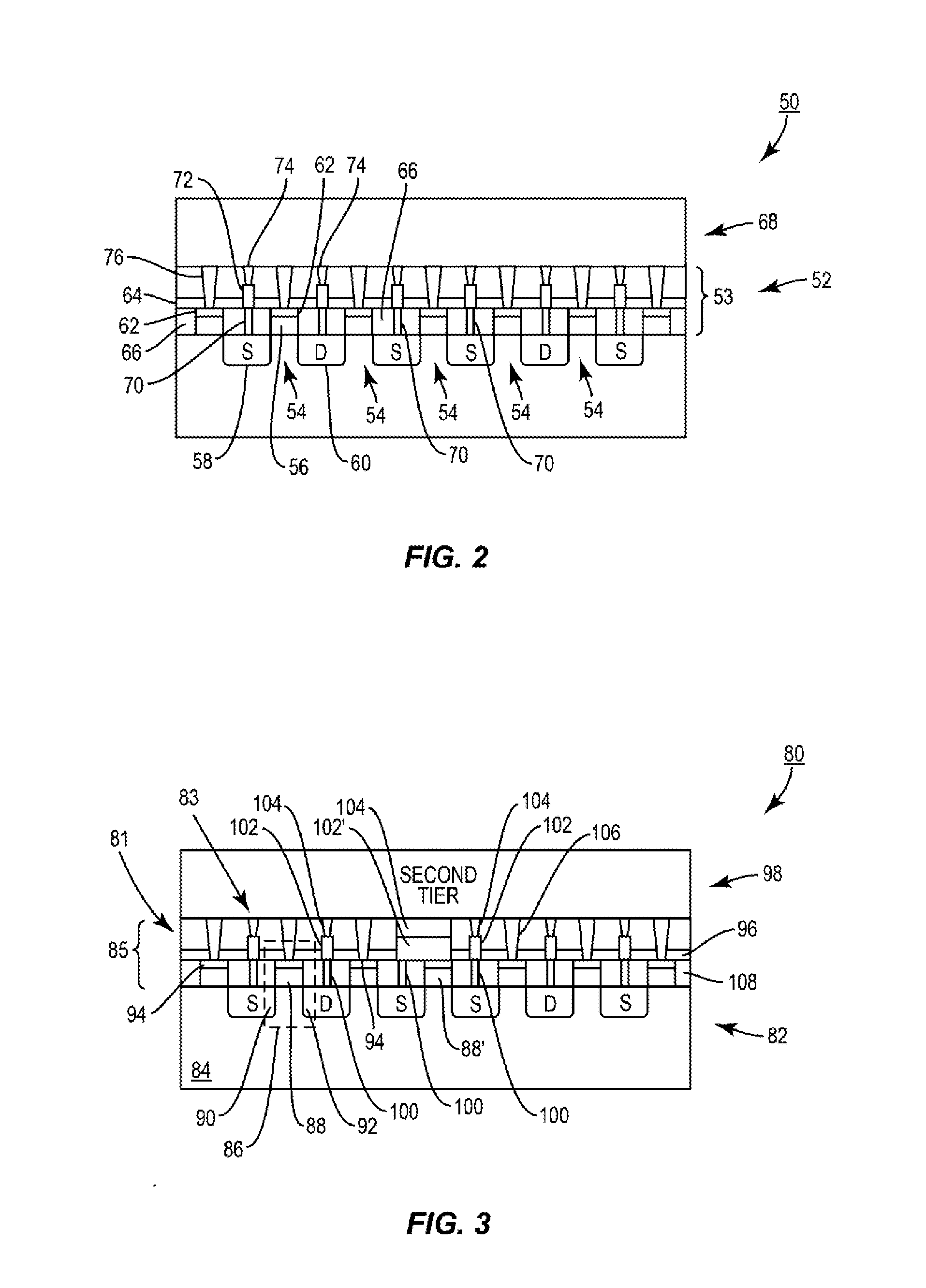
[0021]Aspects disclosed in the detailed description include tie-off structures for middle-of-line (MOL) manufactured integrated circuits, and related methods. As a non-limiting example, the tie-off structure may be used to tie-off a drain or source of a transistor to the gate of the transistor, such as provided in a dummy gate used for isolation purposes. In this regard in one embodiment, a MOL stack is provided that includes a metal gate connection is coupled to a metal layer through a metal structure disposed in and above a dielectric layer above a gate associated with the metal gate connection. By coupling the metal gate connection to the metal lay...


PUM


Abstract

Tie-off structures for middle-of-line (MOL) manufactured integrated circuits, and related methods are disclosed. As a non-limiting example, the tie-off structure may be used to tie-off a drain or source of a transistor to the gate of the transistor, such as provided in a dummy gate used for isolation purposes. In this regard in one aspect, a MOL stack is provided that includes a metal gate connection that is coupled to a metal layer through metal structure disposed in and above a dielectric layer above a gate associated with the metal gate connection. By coupling the metal gate connection to the metal layer, the gate of a transistor may be coupled or “tied-off” to a source or drain element of the transistor. This may avoid the need to etch the metal gate connection provided below the dielectric layer to provide sufficient connectivity between the metal layer and the metal gate connection.

Description

BACKGROUND[0001]I. Field of the Disclosure[0002]The technology of the disclosure relates generally to facilitating interconnections between elements formed from middle-of-line (MOL) processes within an integrated circuit.[0003]II. Background[0004]Computing devices have become commonplace throughout society. The increasing presence of such computing devices has accelerated in part because of the increasing functionality and versatility of such computing devices. The increase in functionality and versatility has been enabled by providing increasingly powerful processing capabilities in small packages as loosely recognized by Moore's Law. The pressures to increase processing capabilities while decreasing the size of the integrated circuits (ICs) have strained conventional manufacturing processes, especially as the node size within ICs has been reduced to low nanometer (nm) dimensions (e.g., <20 nm).[0005]Current semiconductor fabrication of ICs may include front-end-of-line (FEOL), ...

Claims


Application Information

Patent Timeline
Patent Type & Authority Applications(United States)
IPC IPC(8): H01L23/535H01L21/768H01L27/06
CPCH01L23/535H01L21/76895H01L27/0688H01L27/0207H01L2924/0002H01L2924/00
Inventor ZHU, JOHN JIANHONGRIM, KERNSONG, STANLEY SEUNGCHULXU, JEFFREY JUNHAO
Owner QUALCOMM INC
Why Eureka
Try Eureka