Ultraviolet sensor and ultraviolet detecting device

a technology of ultraviolet light and ultraviolet light, which is applied in the direction of diodes, semiconductor devices, radiation control devices, etc., can solve the problems of difficult for the uv sensor using the compound semiconductor difficult for the uv sensor using the silicon photodiodes difficult for the foregoing uv sensor to achieve a sufficient detection sensitivity characteristic, etc., to achieve the effect of easy formation, high detection

Active Publication Date: 2016-03-24
HAMAMATSU PHOTONICS KK
View PDF4 Cites 8 Cited by
  • Summary
  • Abstract
  • Description
  • Claims
  • Application Information

AI Technical Summary

Benefits of technology

[0012]The plurality of first pixel regions and the plurality of second pixel regions may be two-dimensionally disposed and also alternately disposed in a second direction perpendicular to the first direction. This configuration further prevents the light incident to the UV sensor from being incident into only either one of the first and second pixel regions. It also further prevents the light incident to the UV sensor from being disproportionately incident into either one of the first and second pixel regions. Because of these, the UV sensor can achieve higher detection accuracy.
[0013]The filter film may be comprised of a polyparaxylylene resin. In this case, transmittance can be lowered, particularly, in the wavelength region on the short wavelength side such as the UV-C rays, as the detection target wavelength range in the UV region. Since the filter film is disposed on each first pixel region except on each second pixel region, the filter film needs to be formed by patterning. It is easy to implement the patterning of the polyparaxylylene resin. Therefore, the filter film is surely and easily formed on each first pixel region except on each second pixel region.
[0014]The UV sensor may further comprise a condenser lens disposed so as to face the silicon photodiode array, and configured to condense incident light. In this case, it is feasible to enhance light condensing capability in the UV sensor and expand a range where light can be incident into the UV sensor.
[0015]The UV sensor may further comprise a scattering section disposed so as to face the silicon photodiode array, and configured to scatter incident light to output scattered light. This configuration further prevents the light incident to the UV sensor from being incident into only either one of the first and second pixel regions. It also further prevents the light incident to the UV sensor from being disproportionately incident into either one of the first and second pixel regions. Because of these, the UV sensor can achieve higher detection accuracy.
[0016]The UV sensor may further comprise a filter disposed so as to face the silicon photodiode array, and configured to cut light of wavelengths in the visible region traveling toward the silicon photodiode array. A spectral sensitivity characteristic of the avalanche photodiode has a peak in the visible region in general. For this reason, if the quantity of light is higher in the visible region as ambient light than the quantity of light in the UV region, the output from the avalanche photodiode could become saturated. When the output from the avalanche photodiode becomes saturated, it becomes difficult to detect the light in the detection target wavelength range in the UV region. When the filter to cut the light of wavelengths in the visible region is disposed so as to face the silicon photodiode array, it can prevent the output from the avalanche photodiode from becoming saturated.
[0017]The silicon photodiode array may include a silicon semiconductor substrate on which an epitaxial semiconductor layer is formed through an insulating layer, and the avalanche photodiodes may be formed in the epitaxial semiconductor layer. In this case, the thickness of the epitaxial semiconductor layer can be set relatively small, or, to the thickness enough to lower the sensitivity in the visible region, without lowering the sensitivity in the UV region. This can prevent the output from the avalanche photodiode from becoming saturated.

Problems solved by technology

When the intensity of light as detection target is low, it is difficult for the UV sensor using the compound semiconductor to achieve a sufficient detection sensitivity characteristic.
For this reason, it is difficult for the UV sensor using the silicon photodiodes to achieve a sufficient detection sensitivity characteristic in the wavelength region on the short wavelength side such as the UV-C rays.
It is also difficult for the foregoing UV sensor to achieve a sufficient detection sensitivity characteristic, when the intensity of light as detection target is low.

Method used


Image

  • Ultraviolet sensor and ultraviolet detecting device
  • Ultraviolet sensor and ultraviolet detecting device
  • Ultraviolet sensor and ultraviolet detecting device

Examples


Embodiment Construction

[0035]The embodiment of the present invention will be described below in detail with reference to the accompanying drawings. In the description, identical elements or elements with identical functionality will be denoted by the same reference signs, without redundant description.

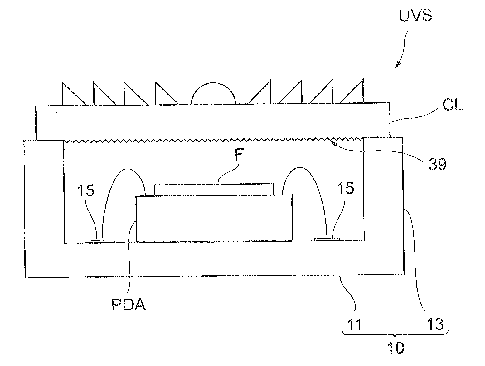
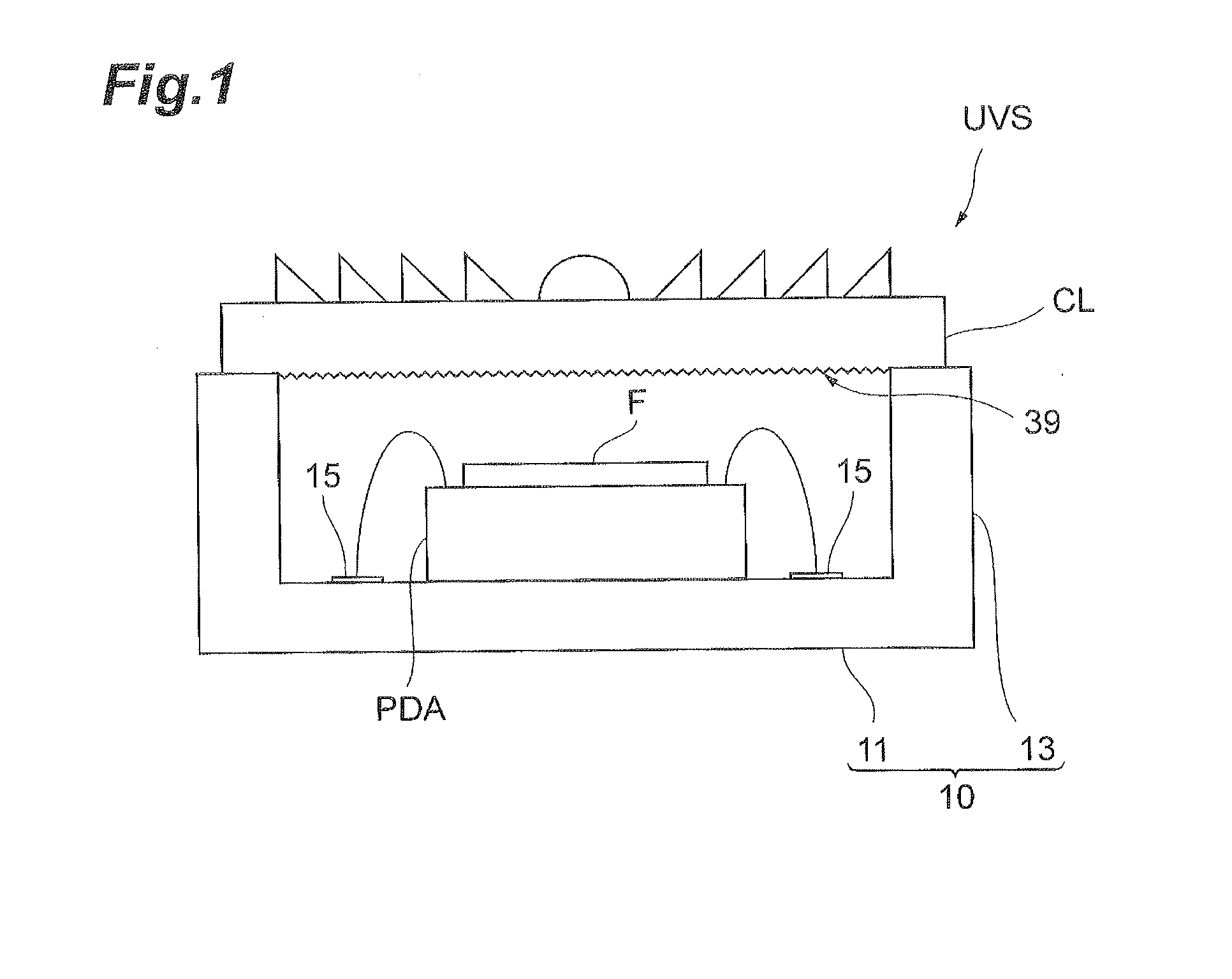
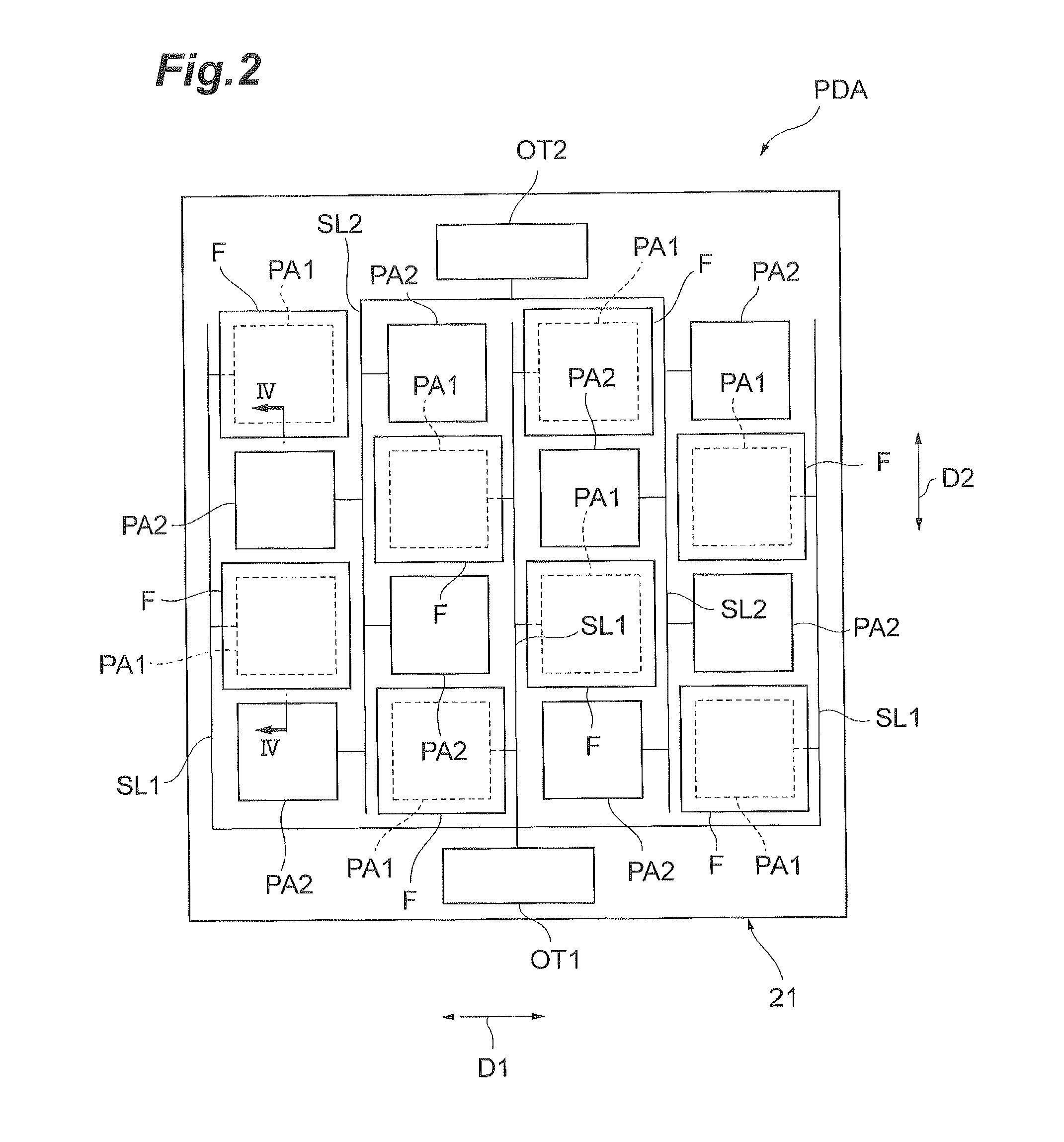
[0036]A configuration of a UV sensor UVS according to the present embodiment will be described with reference to FIGS. 1 to 5. FIG. 1 is a conceptual drawing for explaining a cross-sectional configuration of the UV sensor according to the present embodiment. FIG. 2 is a plan view showing a silicon photodiode array, which the UV sensor according to the present embodiment includes. FIG. 3 is a plan view showing a first pixel region and a second pixel region in the silicon photodiode array shown in FIG. 2. FIG. 4 is a drawing for explaining a cross-sectional configuration along the line IV-IV in FIG. 2. FIG. 5 is a circuit diagram of the UV sensor according to the present embodiment.

[0037]The UV sensor UVS, as ...


PUM


Abstract

An ultraviolet sensor includes a silicon photodiode array having a plurality of first pixel regions and a plurality of second pixel regions. A filter film is disposed on each of the first pixel regions so as to cover each first pixel region, except on each second pixel region. The filter film lowers transmittance in a detection target wavelength range in the ultraviolet region. Each of each first pixel region and each second pixel region includes at least one pixel having an avalanche photodiode to operate in Geiger mode, and a quenching resistor connected in series to the avalanche photodiode. Each of the quenching resistors in the plurality of first pixel regions is connected through a first signal line to a first output terminal. Each of the quenching resistors in the plurality of second pixel regions is connected through a second signal line to a second output terminal.

Description

BACKGROUND OF THE INVENTION[0001]1. Field of the Invention[0002]The present invention relates to an ultraviolet sensor and an ultraviolet detecting device provided with the ultraviolet sensor.[0003]2. Related Background Art[0004]There are known ultraviolet (UV) sensors using compound semiconductors (e.g., cf. Japanese Patent Application Laid-open Publication No. H09-229763). The UV sensor described in the Publication No. H09-229763 includes a sapphire substrate and a compound semiconductor layer formed on the sapphire substrate. This LTV sensor has no sensitivity in a wavelength region longer than a detection target wavelength range in the UV region (e.g., the spectral region C of UV rays (UV-C rays)).[0005]Another known UV sensor is one provided with first and second photodiodes having a spectral sensitivity in a range down to the UV region (e.g., cf. Japanese Unexamined Utility Model Application Publication No. S63-129837). In the UV sensor described in the Publication No. S63-129...

Claims


Application Information

Patent Timeline
Patent Type & Authority Applications(United States)
IPC IPC(8): H01L27/146H01L31/028H01L31/107
CPCH01L27/14621H01L27/14643H01L27/14627H01L31/107H01L27/14636H01L31/028H01L27/14603H01L27/14618H01L27/14625H01L2224/48091H01L2224/48227H01L2924/16195H01L2924/00014
Inventor YAMAMOTO, KOEIHAYATSU, KENZONAGANO, TERUMASAOKUWA, YUKIYAMADA, RYUTA
Owner HAMAMATSU PHOTONICS KK
Why Eureka
Try Eureka