METHODS FOR HIGH-K METAL GATE CMOS WITH SiC AND SiGe SOURCE/DRAIN REGIONS

a metal gate cmos and source/drain technology, applied in the direction of basic electric elements, electrical equipment, semiconductor devices, etc., can solve the problems of dummy gate residue, difficult removal of electrical components, etc., and achieve the effect of simplifying process flow, reducing process cost, and reducing the layer of spacer material

Active Publication Date: 2016-03-24
SEMICONDUCTOR MANUFACTURING INTERNATIONAL (BEIJING) CORP +1
View PDF1 Cites 12 Cited by
  • Summary
  • Abstract
  • Description
  • Claims
  • Application Information

AI Technical Summary

Benefits of technology

[0004]In embodiments of the present invention, a high-k metal gate process is provided in which the hard mask on the PMOS dummy gate structures are retained during source / drain implant. As a result, the spacer material layer can be reduced to lower the process cost. This process also reduces the difference in removal rates of sacrificial gate electrode material in the NMOS region and the PMOS region, simplifying the process flow and improving device performance.

Problems solved by technology

The P+ doped PMOS sacrificial gate electrode material can become much harder to remove, thus, causing dummy gate residue in PMOS region while NMOS dumm gate incompletely removed.

Method used


Image

  • METHODS FOR HIGH-K METAL GATE CMOS WITH SiC AND SiGe SOURCE/DRAIN REGIONS
  • METHODS FOR HIGH-K METAL GATE CMOS WITH SiC AND SiGe SOURCE/DRAIN REGIONS
  • METHODS FOR HIGH-K METAL GATE CMOS WITH SiC AND SiGe SOURCE/DRAIN REGIONS

Examples


Embodiment Construction

[0028]The description below is presented with reference to a series of drawing figures enumerated above. These diagrams are merely examples, and should not unduly limit the scope of the claims herein. In connection with the various aspects illustrated and described, one of ordinary skill in the art would recognize other variations, modifications, and alternatives.

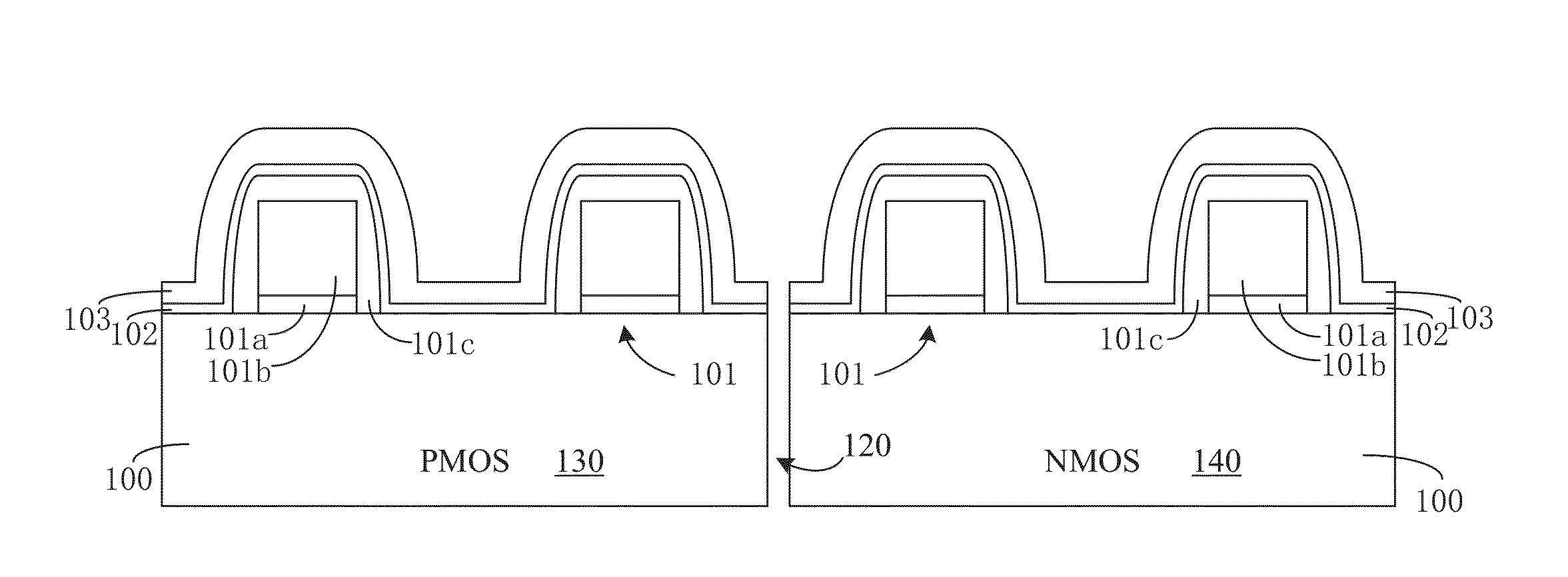
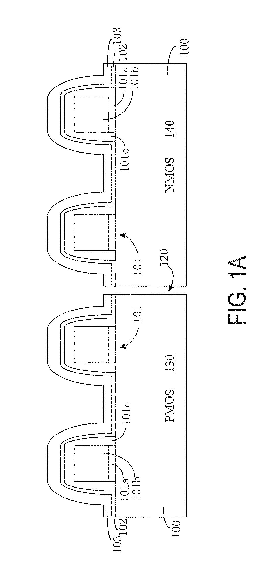
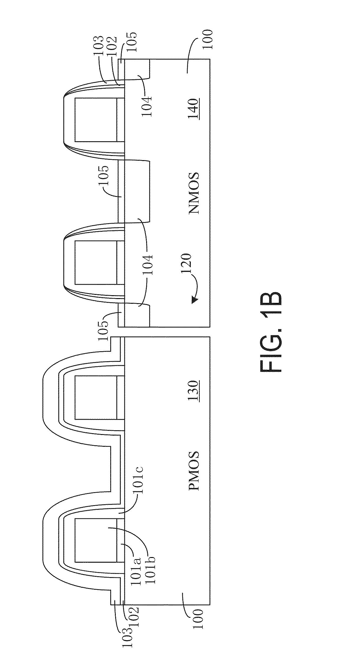
[0029]FIGS. 1A-1G are cross-sectional views showing a method for forming semiconductor devices according to an exemplary embodiment of the present invention.

[0030]First, as shown in FIG. 1A, a PMOS device and an NMOS device are formed in a semiconductor substrate 100. Semiconductor substrate 100 can include such material as undoped silicon, doped with impurities of silicon, silicon on insulator (SOI), stacked insulator silicon (SSOI), silicon-germanium-on-insulator laminate (S—SiGeOI), silicon-germanium-on-insulator (SiGeOI) and germanium on insulator (GeOI), and the like. Merely as an example, in the present embodiment the...


PUM


Abstract

A method of manufacturing a semiconductor device includes forming a PMOS region and an NMOS region in a semiconductor substrate, forming dummy gate structures in the PMOS and NMOS regions, and forming a gate hard mask layer overlying top portions and sidewalls of the dummy gate structures. The method includes forming silicon carbon regions embedded in the semiconductor substrate on both sides of the dummy gate structure in the NMOS region, removing the hard mask layer on top of the dummy gate in the NMOS region, and forming silicon germanium regions embedded in the semiconductor substrate on both sides of the dummy gate structure in the PMOS region. After forming the silicon carbon regions and the silicon germanium regions, while retaining the hard mask layer on top of the dummy gates in the PMOS region, performing ion implant to form source/drain regions in the NMOS region and the PMOS region.

Description

BACKGROUND OF THE INVENTION[0001]Embodiments of present invention relate to semiconductor manufacturing processes. More particularly, embodiments of the present invention provide improved methods to realize a high-k metal gate device structure.[0002]In the next generation of integrated circuit manufacturing process, complementary metal oxide semiconductor (CMOS) devices are often implemented in a high-k metal gate device structure. An example of such process includes forming dummy gate structures on a first semiconductor substrate. The dummy gate structure includes a sacrificial gate layer and a sacrificial gate dielectric material layer. A silicon germanium (SiGe) layer is embedded in the semiconductor substrate on both sides of the dummy gate of the PMOS portion, and then a silicon carbon (SiC) layer is embedded on a semiconductor substrate on both sides of the dummy gate structure of the NMOS portion of the CMOS. Then, after spacers are formed, ion implantation is carried out to ...

Claims


Application Information

Patent Timeline
Patent Type & Authority Applications(United States)
IPC IPC(8): H01L29/165H01L29/66
CPCH01L29/165H01L29/66553H01L29/66545H01L21/823814H01L29/51H01L29/66636H01L29/78
Inventor MAO, GANG
Owner SEMICONDUCTOR MANUFACTURING INTERNATIONAL (BEIJING) CORP
Why Eureka
Try Eureka