
Finfet with heterojunction and improved channel control

a technology of heterojunction and finfet, which is applied in the direction of semiconductor devices, electrical apparatus, transistors, etc., can solve the problems of leakage through the middle of the fin, difficulty in implementation, and limited depth of the electric field generated by the gate control voltage, so as to achieve more powerful circuits, components and systems, and improve chip yields

Active Publication Date: 2016-03-24
SYNOPSYS INC
View PDF6 Cites 17 Cited by
  • Summary
  • Abstract
  • Description
  • Claims
  • Application Information

AI Technical Summary

Benefits of technology

The patent text discusses the problem of reduced gate control voltage in FinFET transistors with different crystalline materials in the fin and fin support. The text proposes a solution to improve chip yields, make circuits, components, and systems more dense, and make them more powerful. In summary, the patent aims to create stronger and more reliable products with better performance using different crystalline materials.

Problems solved by technology

Such issues discourage FinFET transistors made from different crystalline materials in the fin and fin support.
But even with such narrow fins, the electric field generated by the gate control voltage can be limited in depth and may not extend sufficiently into the cross-sectional middle of the fin.
In the off-state, this causes leakage through the middle of the fin.
Manufacturers can reduce this problem by narrowing the fin further, but this solution is difficult to implement because the mechanical instability and line edge roughness of such a narrow fin can cause yield loss.
Fringing electric fields generated from the gate near a crystalline fin support are not expected to solve the issue of decreased gate voltage control in the middle of the fin.

Method used


Image

  • Finfet with heterojunction and improved channel control
  • Finfet with heterojunction and improved channel control
  • Finfet with heterojunction and improved channel control

Examples


Embodiment Construction

[0083]The following description is presented to enable any person skilled in the art to make and use the invention, and is provided in the context of a particular application and its requirements. Various modifications to the disclosed embodiments will be readily apparent to those skilled in the art, and the general principles defined herein may be applied to other embodiments and applications without departing from the spirit and scope of the present invention. Thus, the present invention is not intended to be limited to the embodiments shown, but is to be accorded the widest scope consistent with the principles and features disclosed herein.

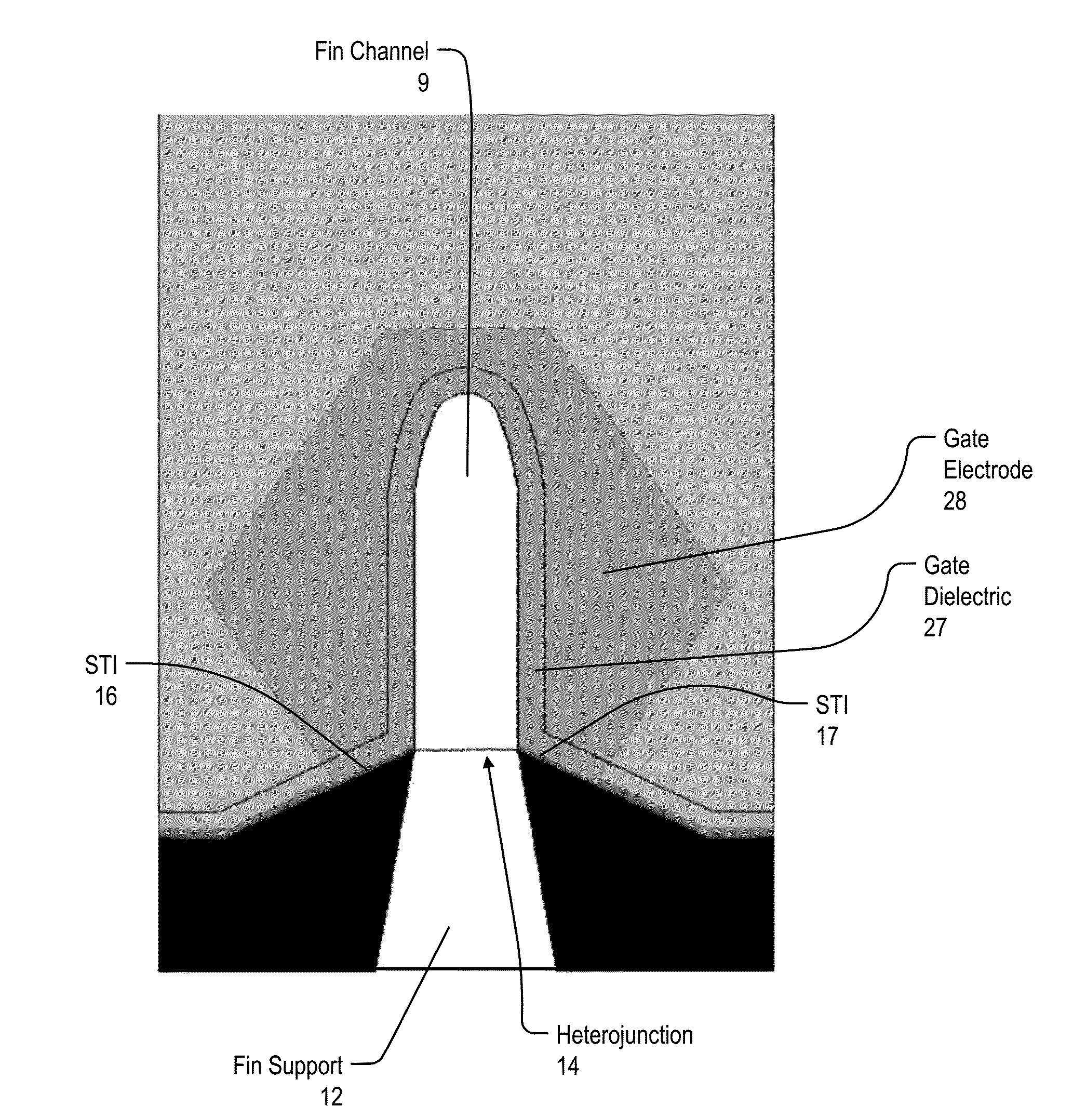
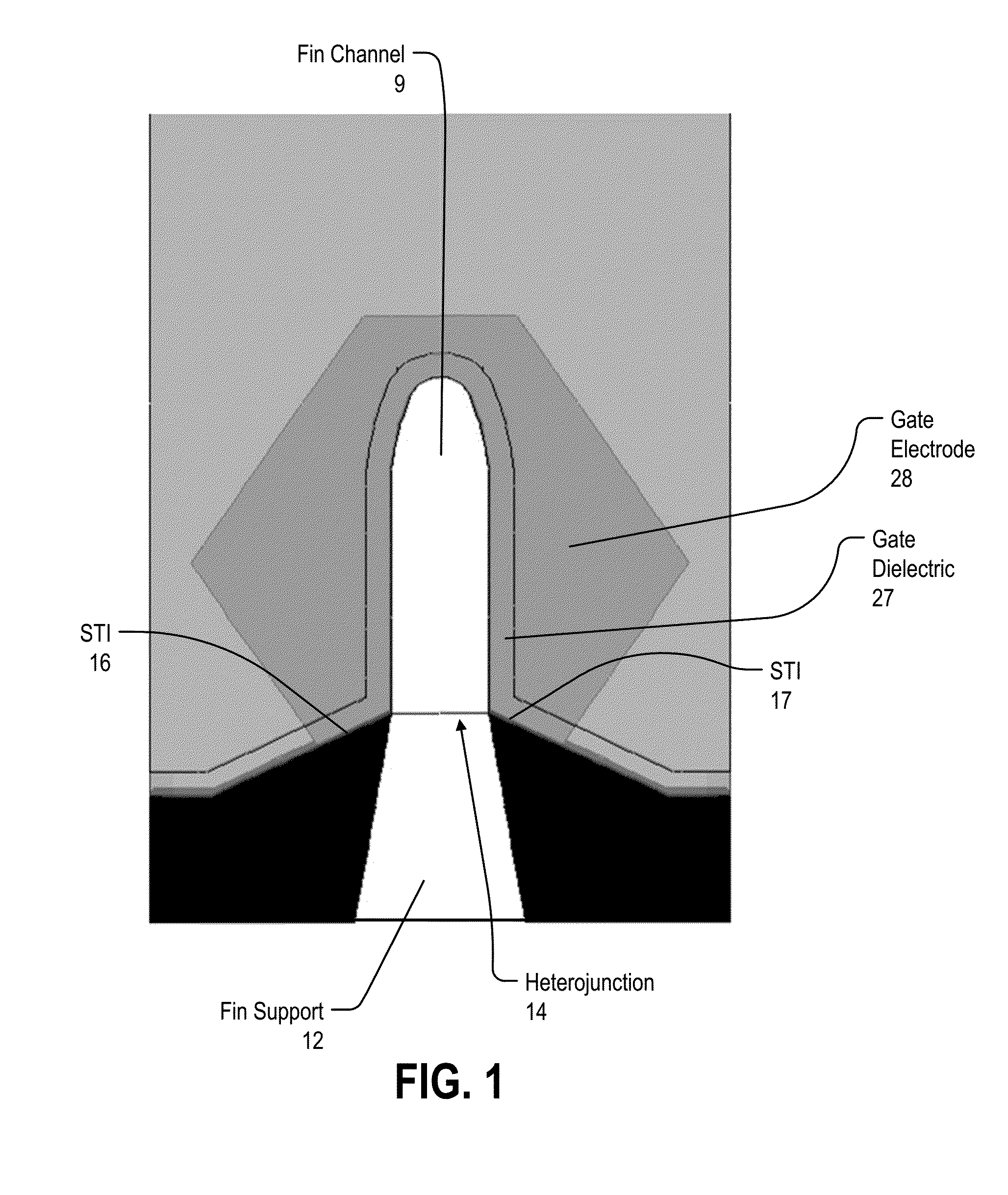
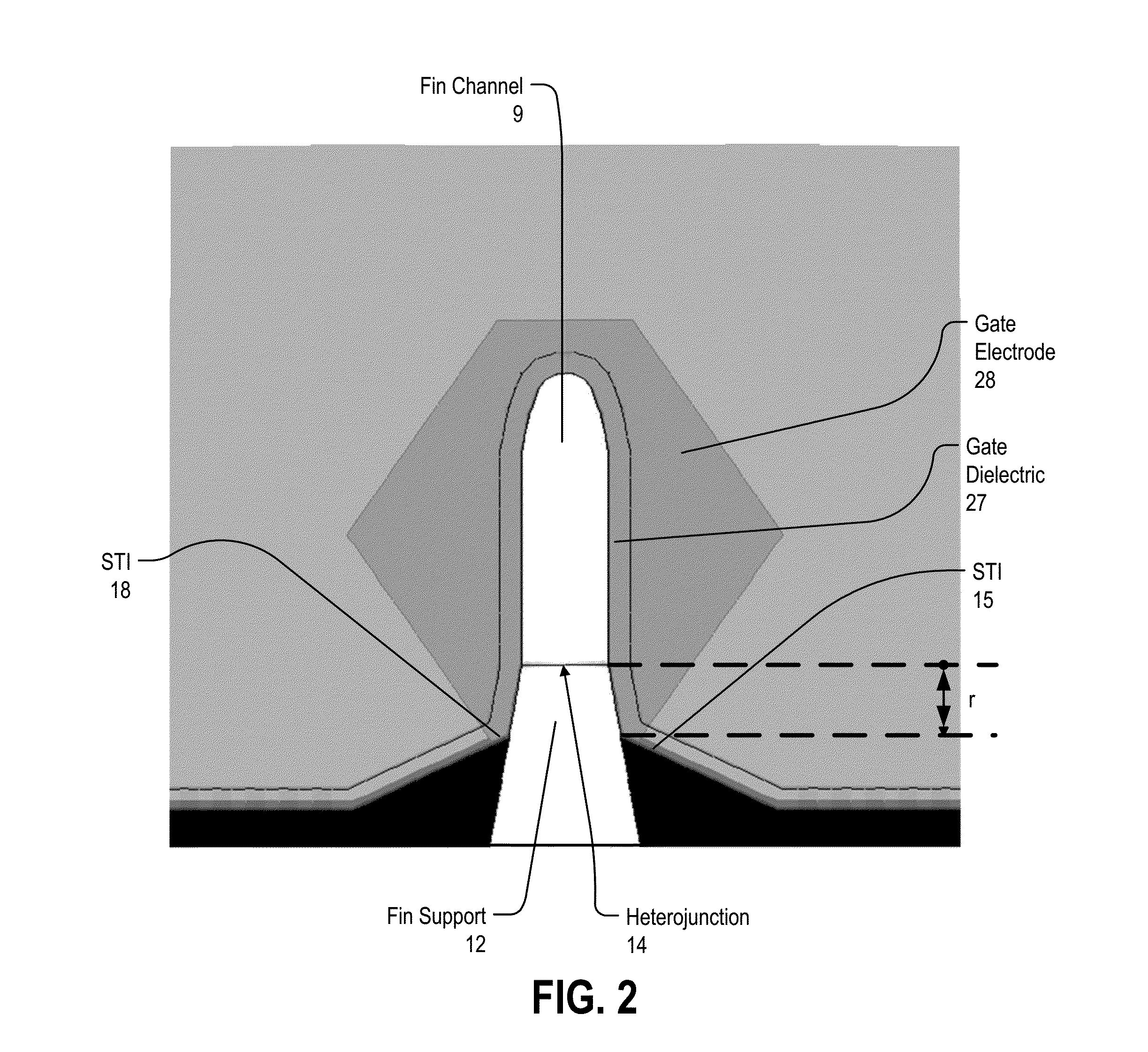
[0084]FIG. 1 illustrates a simplified FinFET transistor with a crystalline fin and a crystalline fin support.

[0085]The figure is a cross-section of the channel portion of a FinFET, with current going in a direction in a Z-direction perpendicular to the page. The portion of the fin 9 shown is the channel region, with source and drain regions of ...


PUM


Abstract

Roughly described, a computer program product describes a transistor with a fin, a fin support, a gate, and a gate dielectric. The fin includes a first crystalline semiconductor material which includes a channel region of the transistor between a source region of the first transistor and a drain region of the transistor. The fin is on a fin support. The fin support includes a second crystalline semiconductor material different from the first crystalline semiconductor material. The first crystalline semiconductor material of the fin and the second crystalline semiconductor material of the fin support form a first heterojunction in between. A gate, gate dielectric, and / or isolation dielectric can be positioned to improve control within the channel.

Description

CROSS REFERENCES[0001]This application is a Continuation of PCT International Application No. PCT / US14 / 44259, filed 26 Jun. 2014, entitled “FINFET WITH HETEROJUNCTION AND IMPROVED CHANNEL CONTROL,” by Victor Moroz, Stephen L. Smith and Qiang Lu, (Atty. Docket No. SYNP 2336-1), which application claims the benefit of U.S. Provisional Application No. 61 / 839,534, filed 26 Jun. 2013, entitled “FINFET WITH CHANNEL / SRB HETEROJUNCTION AND RECESSED STI,” by Victor Moroz, Stephen L. Smith and Qiang Lu, (Atty. Docket No. SYNP 2336-0), both of which are incorporated by reference herein in their entirety.FIELD OF THE INVENTION[0002]The invention relates to semiconductor fabrication, and more particularly to a technique for improved gate control of FinFETs with crystalline fins and crystalline fin supports.BACKGROUND[0003]As integrated circuit technologies continue to push into higher densities, a number of transistor types have become popular which involve one or more narrow channel structures ...

Claims


Application Information

Patent Timeline
Patent Type & Authority Applications(United States)
IPC IPC(8): H01L29/78H01L27/02H01L27/092
CPCH01L29/7848H01L27/0924H01L27/0207H01L29/785H01L29/66795H01L29/1054
Inventor MOROZ, VICTORSMITH, STEPHEN, L.LU, QIANG
Owner SYNOPSYS INC
Learn More