Thin-film piezoelectric material element, method of manufacturing the same, head gimbal assembly, hard disk drive, ink jet head, variable focus lens and sensor

a piezoelectric material and thin film technology, applied in the direction of inking apparatus, instruments, lenses, etc., can solve the problems of increasing materials costs, needing another cost, and likely reducing the yield of piezoelectric laminated materials, so as to achieve the effect of reducing cost and without loss of mass production capability

Active Publication Date: 2016-03-31
SAE MAGNETICS (HK) LTD
View PDF8 Cites 11 Cited by
  • Summary
  • Abstract
  • Description
  • Claims
  • Application Information

AI Technical Summary

Benefits of technology

[0043]As explained above in detail, in the thin-film piezoelectric material element, method of manufacturing the same, head gimbal assembly, hard disk drive, ink jet head, variable focus lens and sensor, curve and crooked displacement are able to be suppressed even the piezoelectric laminated material having a single layer, and the thin-film piezoelectric material element enhanced a close adhesion of thin-film is able to be manufactured a without loss of mass production capability and cost decreasing effect.

Problems solved by technology

However, in case of the method of manufacturing disclosed in the Patent Document 2, two substrates, which a plurality of thin-films are formed, need to be prepared, so there is a problem which a cost for materials increase.
Further, a specific instrument and apparatus are needed when the substrates are adhered each other, so it needs another cost for that.
Furthermore, a yield for the piezoelectric laminated material is likely to be decreased by performing adhering process, and two substrates are likely to peel off each other.
Accordingly, in case of the method of manufacturing disclosed in the Patent Document 2, both improvement of the mass production capability and lowering of the manufacturing cost are difficult.
Further, adhesive layer is likely to peel off each other and is likely to form a gap or crack in the piezoelectric laminated material.
Therefore, curves (or bowing) of the piezoelectric laminated material are not able to be suppressed sufficiently in these conventional technologies.
Further, the supplementary actuator used for hard disk drive does not need the crooked displacement, the crooked displacement are not able to be suppressed in these conventional technologies.

Method used


Image

  • Thin-film piezoelectric material element, method of manufacturing the same, head gimbal assembly, hard disk drive, ink jet head, variable focus lens and sensor
  • Thin-film piezoelectric material element, method of manufacturing the same, head gimbal assembly, hard disk drive, ink jet head, variable focus lens and sensor
  • Thin-film piezoelectric material element, method of manufacturing the same, head gimbal assembly, hard disk drive, ink jet head, variable focus lens and sensor

Examples


modified example 2

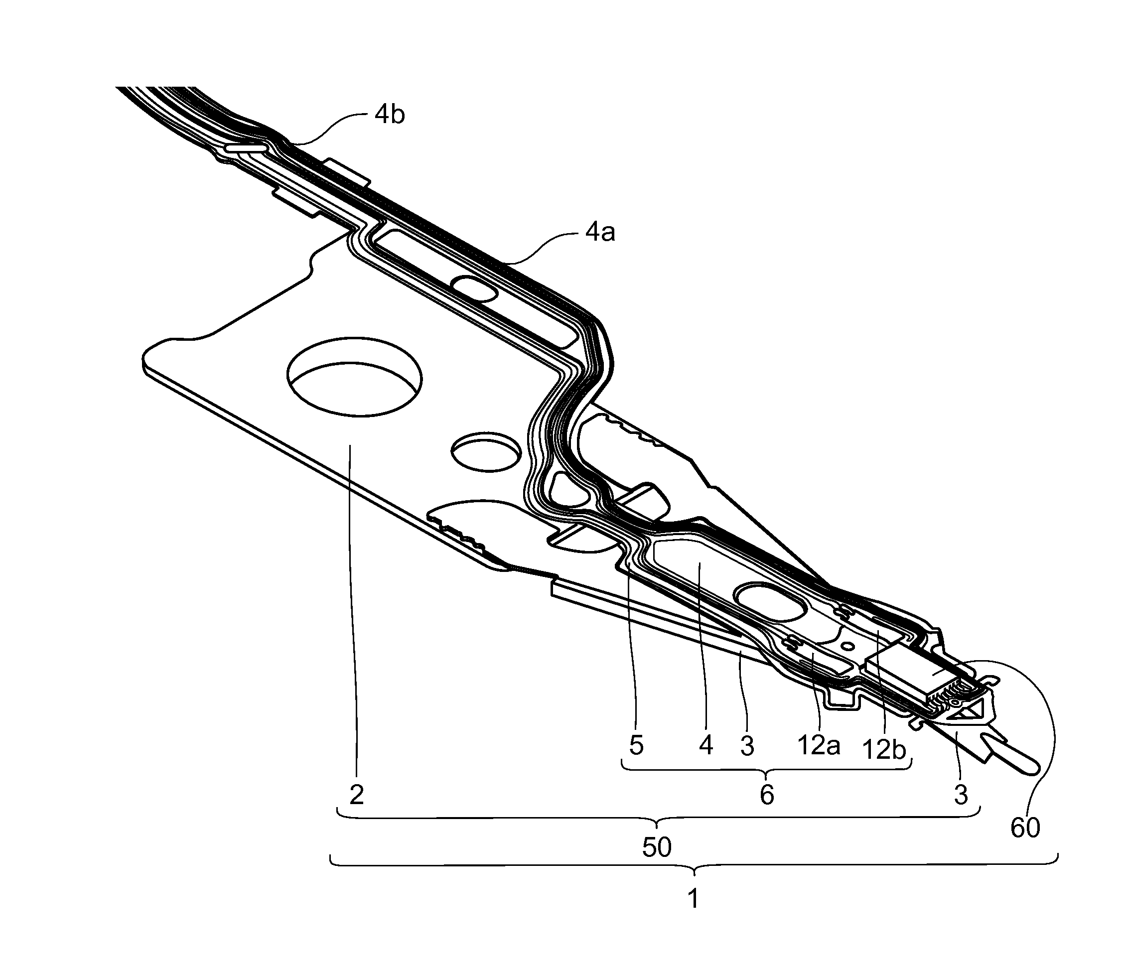
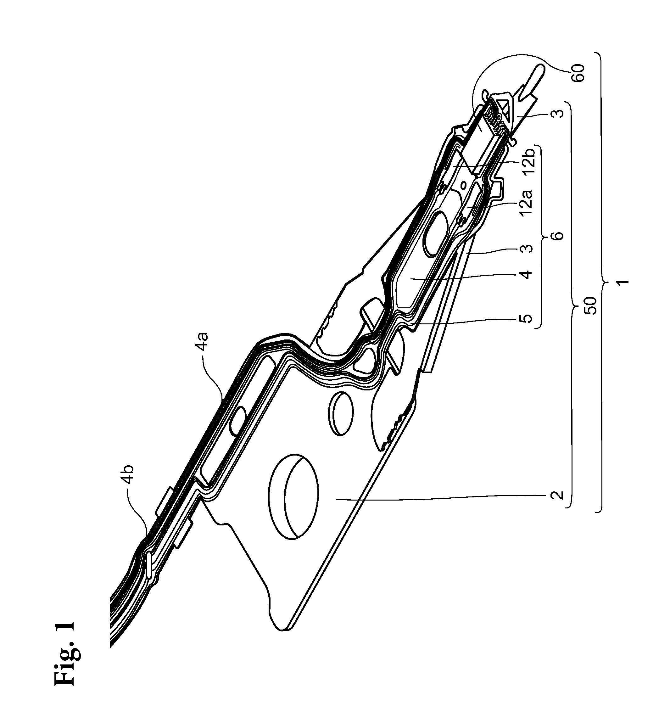
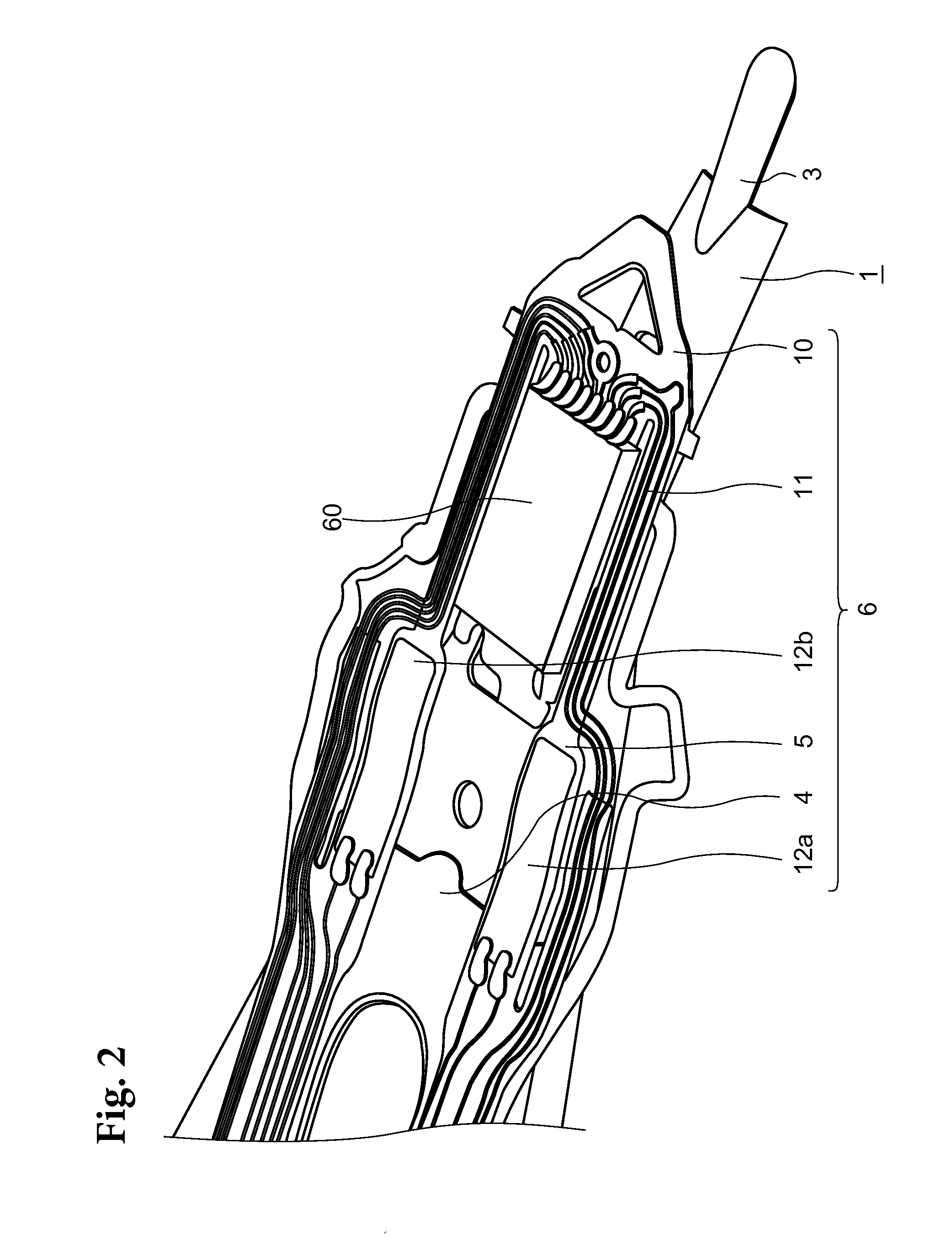
[0151]Subsequently, a thin-film piezoelectric material element 112b according to the modified example will be explained with reference to FIG. 22 to FIGS. 24 (A) and 24 (B). FIG. 22 is a sectional view, similar with FIG. 5, showing a part of the flexure 6 which the thin-film piezoelectric material element 112b according to a modified example is fixed. FIG. 23 is a sectional view showing a part of the thin-film piezoelectric material element 112b with enlargement from the piezoelectric material film 13 to the stress balancing film 14. FIG. 24 (A) is a sectional view, similar with FIG. 6, showing a principal part of FIG. 23 with enlargement, (B) is a sectional view showing a principal part of (A) with enlargement.

[0152]The thin-film piezoelectric material element 112b is different in that it has an upper electrode film 127 in place of the upper electrode film 27, as compared with the above-described thin-film piezoelectric material element 12b. The upper electrode film 127 is differen...

example

[0160]Present inventors form the piezoelectric material film 13 according to the-above described piezoelectric material deposition condition, after that, they form the stress balancing film 14 using alloy material including Fe, Co and Mo, thereby they form the thin-film piezoelectric material element 12b. As a result, curve of the element is decreased largely, and crooked displacement along to the thickness direction is able to be suppressed. Further, they form the thin-film piezoelectric material element not having the stress balancing film 14, they compared displacements (stroke sensitivities) per unit voltage along the longitudinal direction between both the thin-film piezoelectric material element, it is able to be confirmed that the stroke sensitivity of the former (the thin-film piezoelectric material element 12b having the stress balancing film 14) is improved about 40% than the stroke sensitivity of the latter.

[0161]Further, as a result of the X-ray Diffraction (XRD) measure...


PUM

PropertyMeasurementUnit
thicknessaaaaaaaaaa
thicknessaaaaaaaaaa
thicknessaaaaaaaaaa

Abstract

A thin-film piezoelectric material element includes a lower electrode film, a piezoelectric material film, and an upper electrode film, the lower electrode film, the piezoelectric material film and the upper electrode film are laminated sequentially. An upper surface of the piezoelectric material film is a concavity and convexity surface having a convex part and a concave part, the convex part is a curved surface convexly projected, and the concave part is a curved surface concavely hollowed, the upper electrode film is formed on the concavity and convexity surface. The thin-film piezoelectric material element has a stress balancing film formed with a material having an internal stress capable of cancelling an element stress, the stress balancing film is formed on the upper electrode film.

Description

CROSS-REFERENCE TO RELATED APPLICATIONS[0001]This application is based upon and claims the benefit of priority from Japanese Patent Application No. 2014-198676, filed Sep. 29, 2014 and Japanese Patent Application No. 2014-239589, filed Nov. 27, 2014, the entire contents of which are incorporated herein by reference.BACKGROUND[0002]1. Field of the Invention[0003]The present invention relates to a thin-film piezoelectric material element which has a piezoelectric material and electrodes having thin-film like shape and method of manufacturing the same, head gimbal assembly, hard disk drive, ink jet head, variable focus lens and sensor having the thin-film piezoelectric material element.[0004]2. Related Background Art[0005]A hard disk drive has a large recording capacity and is used as the heart of a storage device. The hard disk drive records and reproduces data to / from a hard disk (recording medium) by a thin-film magnetic head. A part, which the thin-film magnetic head is formed, is ...

Claims


Application Information

Patent Timeline
Patent Type & Authority Applications(United States)
IPC IPC(8): H01L41/053G11B5/48H01L41/113G02B3/14H01L41/08B41J2/14
CPCH01L41/0536H01L41/0805B41J2/14233H01L41/1132G02B3/14G11B5/483B41J2202/03G11B5/4873H10N30/10516H10N30/302H10N30/074B41J2/14G11B5/5552G02B7/04H10N30/886H10N30/501H10N30/1051
Inventor XIONG, WEINOGUCHI, TAKAOIITSUKA, DAISUKE
Owner SAE MAGNETICS (HK) LTD
Why Eureka
Try Eureka