Quantum cascade laser

a laser and quantum cascade technology, applied in the direction of laser details, semiconductor lasers, electrical devices, etc., can solve the problems of decreasing production yield and durability (mechanical strength), and achieve the effects of increasing etching depth, increasing production yield and durability (mechanical strength), and relatively large thickness of stacked semiconductor layers

Active Publication Date: 2016-03-31
SUMITOMO ELECTRIC IND LTD
View PDF2 Cites 8 Cited by
  • Summary
  • Abstract
  • Description
  • Claims
  • Application Information

AI Technical Summary

Benefits of technology

[0006]The etching of the stacked semiconductor layer is performed until the etching reaches the substrate. The thickness of the stacked semiconductor layer is relatively large, and thus the etching depth increases. Therefore, when the distributed Bragg reflector and the QCL mesa waveguide are formed by etching, the production yield and the durability (mechanical strength) decrease due to, for example, damage to the side surface of the distributed Bragg reflector.

Problems solved by technology

Therefore, when the distributed Bragg reflector and the QCL mesa waveguide are formed by etching, the production yield and the durability (mechanical strength) decrease due to, for example, damage to the side surface of the distributed Bragg reflector.

Method used


Image

  • Quantum cascade laser
  • Quantum cascade laser
  • Quantum cascade laser

Examples


first embodiment

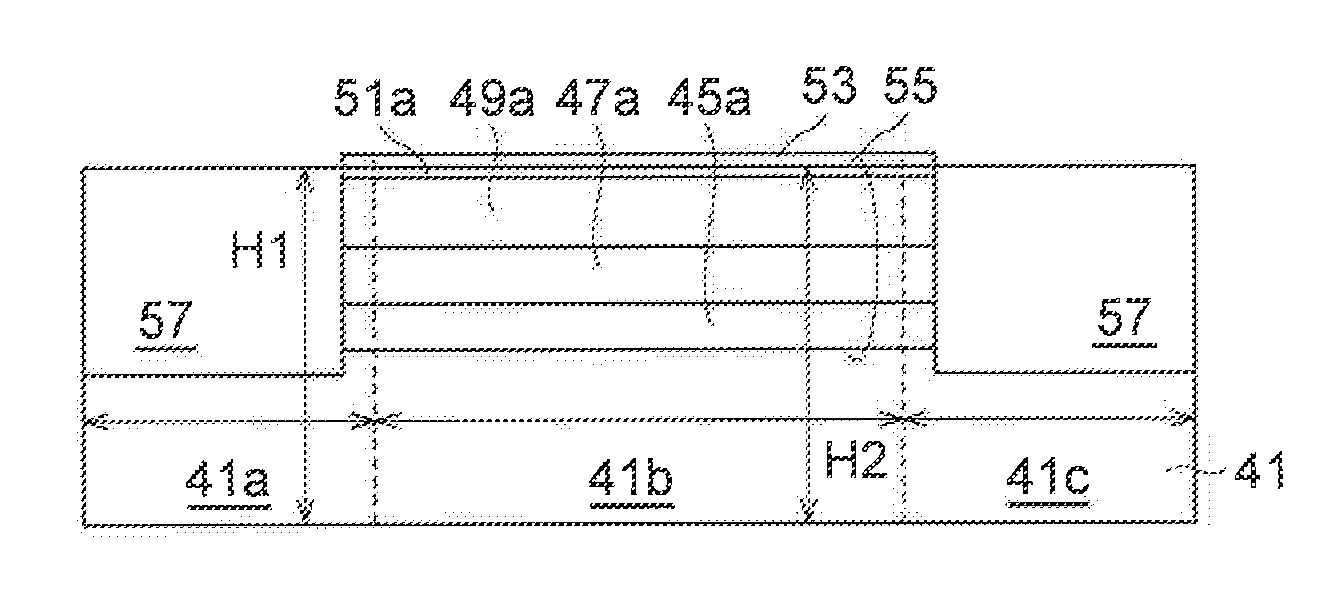
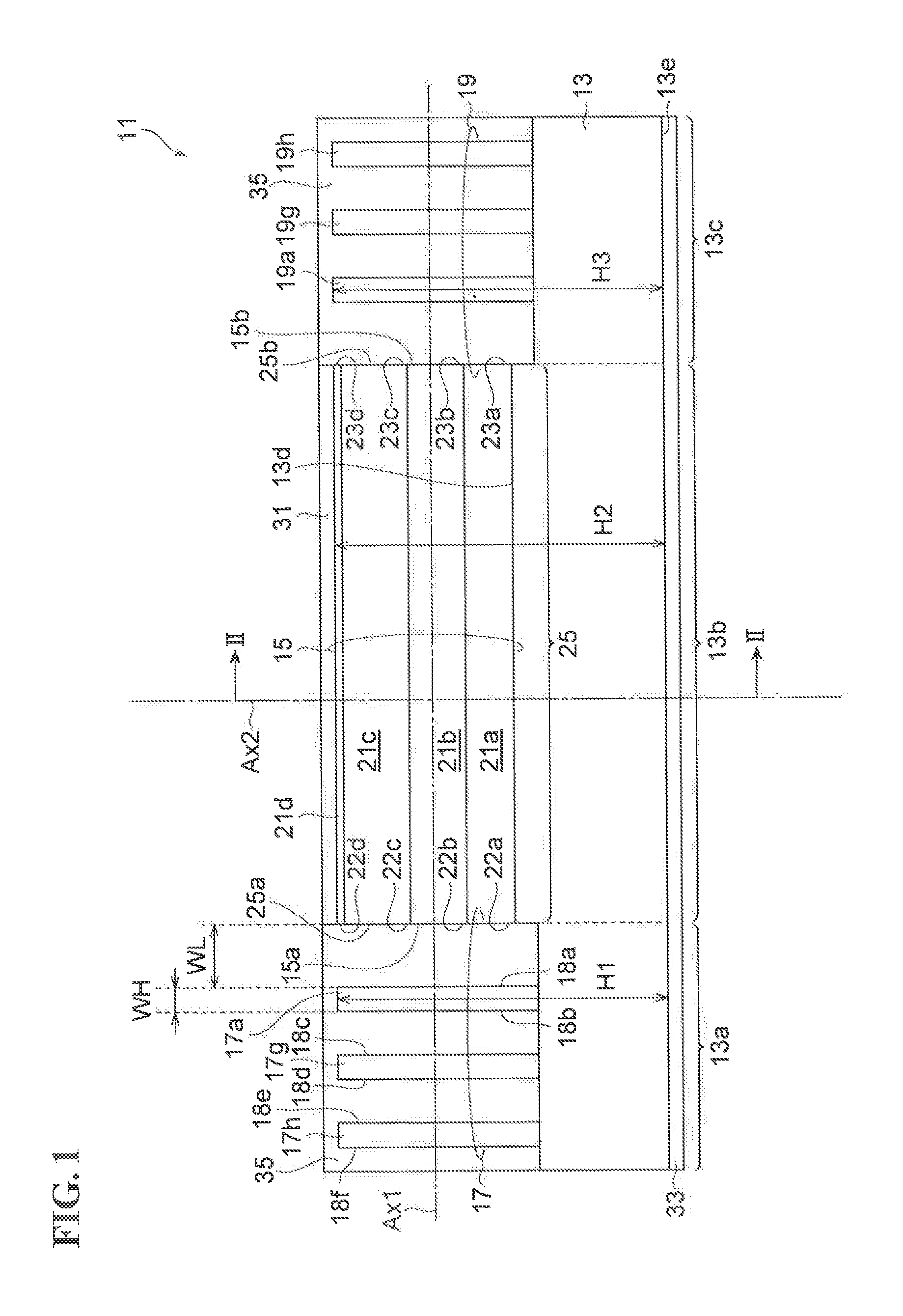
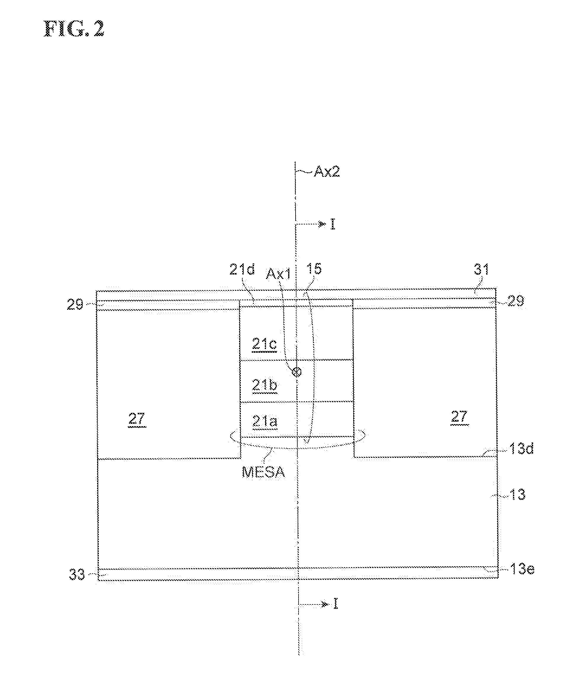
[0053]FIG. 1 schematically illustrates a quantum cascade laser (QCL) according to this embodiment. FIG. 1 illustrates a quantum cascade laser 11 including a distributed Bragg reflection structure. FIG. 1 is a sectional view taken in a direction in which an optical waveguide of the quantum cascade laser 11 extends. The quantum cascade laser 11 includes a substrate 13, a stacked semiconductor layer 15, a distributed Bragg reflection structure 17, and another distributed Bragg reflection structure 19. The substrate 13 includes a first region 13a, a second region 13b, and a third region 13c. The first region 13a, the second region 13b, and the third region 13c are arranged along a first axis Ax1 that indicates a direction in which the optical waveguide of the quantum cascade laser 11 extends. The substrate 13 has a principal surface 13d and a back surface 13e. Thus, each of the first region 13a, the second region 13b, and the third region 13c also has the principal surface 13d and the b...

second embodiment

[0105]A method for producing a quantum cascade laser will be described with reference to FIG. 4A to FIG. 12D. In FIG. 4A to FIG. 12D, FIGS. 4A, 5A, 6A, 7A, 8A, 9A, 10A, 11A, and 12A are sectional views in a stacked semiconductor layer to be a laser main body, the sectional views being taken along a line (for example, in FIG. 4A, line IVa-IVa of FIG. 4C) perpendicular to a direction in which an optical waveguide extends. FIGS. 4B, 5B, 6B, 7B, 8B, 9B, 10B, 11B, and 12B are sectional views in a semiconductor wall of a distributed Bragg reflection structure, the sectional views being taken along a line (for example, in FIG. 4B, line IVb-IVb of FIG. 4C) perpendicular to a direction in which an optical waveguide extends. FIGS. 4C, 5C, 6C, 7C, 8C, 9C, 10C, 11C, and 12C are sectional views illustrating an optical waveguide, the sectional views being taken along a line (for example, in FIG. 4C, line IVc-IVc of FIG. 4A) that extends in a direction in which the optical waveguide extends. FIGS....

third embodiment

[0116]FIG. 13 illustrates a quantum cascade laser 11a. The quantum cascade laser 11a includes a distributed Bragg reflection structure 81 (83) instead of the distributed Bragg reflection structure 17 (19) of the quantum cascade laser 11. The distributed Bragg reflection structure 81 (83) includes one or more semiconductor walls 81b (83b) that are arranged away from the end facet 15a (15b) of the stacked semiconductor layer 15. The end facet 15a (15b) of the stacked semiconductor layer 15 and the semiconductor walls 81b (83b) are arranged along the first axis Ax1 to constitute the distributed Bragg reflection structure 81 (83). The distance D3 between the upper ends of the semiconductor walls 81b (83b) and the back surface of the substrate 13 is larger than the distance D2 between the upper surface of the stacked semiconductor layer 15 and the back surface of the substrate 13. The semiconductor walls 81b (83b) are extended in the Ax2 direction with a predetermined distance so that li...


PUM


Abstract

A quantum cascade laser includes a substrate having a principal surface including first and second regions arranged along a first axis; a laser structure disposed on the principal surface in the second region, the laser structure having an end facet intersecting the first axis, the laser structure including a stripe-shaped stacked semiconductor layer extending along the first axis; and a distributed Bragg reflection structure disposed on the principal surface in the first region, the distributed Bragg reflection structure including a semiconductor wall made of a single semiconductor material, the distributed Bragg reflection structure being optically coupled to the end facet of the laser structure. The semiconductor wall has first and second side surfaces that intersect the first axis and extend along a second axis intersecting the principal surface. The semiconductor wall is located away from the end facet of the laser structure.

Description

BACKGROUND OF THE INVENTION[0001]1. Field of the Invention[0002]The present invention relates to a quantum cascade laser.[0003]2. Description of the Related Art[0004]Jpn. J. Appl. Phys., vol. 39, pp. L1297-1299, 2000 (Non-Patent Document 1), Journal of Modern Optics, vol. 52, No. 16, pp. 2303-2308, 2005 (Non-Patent Document 2), and Jpn. J. Appl. Phys., vol. 39, pp. 3406-3409, 2000 (Non-Patent Document 3) disclose quantum cascade lasers. In particular, Non-Patent Document 2 discloses a quantum cascade laser (QCL) including a mesa waveguide and a distributed Bragg reflector constituted by semiconductor / air. The distributed Bragg reflector reflects light emitted from the mesa waveguide.SUMMARY OF THE INVENTION[0005]In the production of the quantum cascade laser (QCL) including the distributed Bragg reflector as disclosed in Non-Patent Document 2, first, a stacked semiconductor layer for forming a mesa waveguide and a distributed Bragg reflector is grown on a substrate. Subsequently, th...

Claims


Application Information

Patent Timeline
Patent Type & Authority Applications(United States)
IPC IPC(8): H01S5/34H01S5/125H01S5/22
CPCH01S5/3402H01S5/125H01S5/22H01S5/0202H01S5/02476H01S5/2224H01S2301/176H01S5/0234H01S5/0237
Inventor HASHIMOTO, JUN-ICHI
Owner SUMITOMO ELECTRIC IND LTD
Why Eureka
Try Eureka