Fabricating metal source-drain stressor in a mos device channel

a technology of metal source and stressor, which is applied in the direction of basic electric elements, semiconductor devices, electrical equipment, etc., can solve the problems of void formation, stress due to thermal expansion coefficient difference between silicide and substrate or channel, etc., and achieve low contact resistance and improved tensile stress

Inactive Publication Date: 2016-05-12
SAMSUNG ELECTRONICS CO LTD
View PDF0 Cites 10 Cited by
  • Summary
  • Abstract
  • Description
  • Claims
  • Application Information

AI Technical Summary

Benefits of technology

[0005]The exemplary embodiment provides methods and systems for fabricating a metal source-drain stressor in a MOS device channel having improved tensile stress. Aspects of exemplary embodiment include forming a recess in source and drain areas; forming a metal contact layer on surfaces of the recess that achieves low contact resistivity; forming a metallic diffusion barrier over the metal contact layer; forming a layer M as an intimate mixture of materials A and B that substantially fills the recess; capping the layer M with a capping layer so that layer M is fully encapsulated and the capping layer prevents diffusion of A and B; and forming a compound AxBy within the layer M via a thermal reaction resulting in a reacted layer M comprising the metal source-drain stressor.

Problems solved by technology

However, stress due to difference in thermal expansion coefficient between silicide and substrate or channel is limited.
If the available volume is constrained, for example by encapsulation, although some tensile strain may be developed, however, the main result in this case is the formation of voids.

Method used


Image

  • Fabricating metal source-drain stressor in a mos device channel
  • Fabricating metal source-drain stressor in a mos device channel
  • Fabricating metal source-drain stressor in a mos device channel

Examples


Embodiment Construction

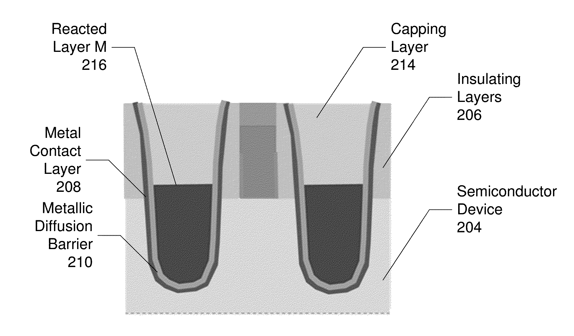
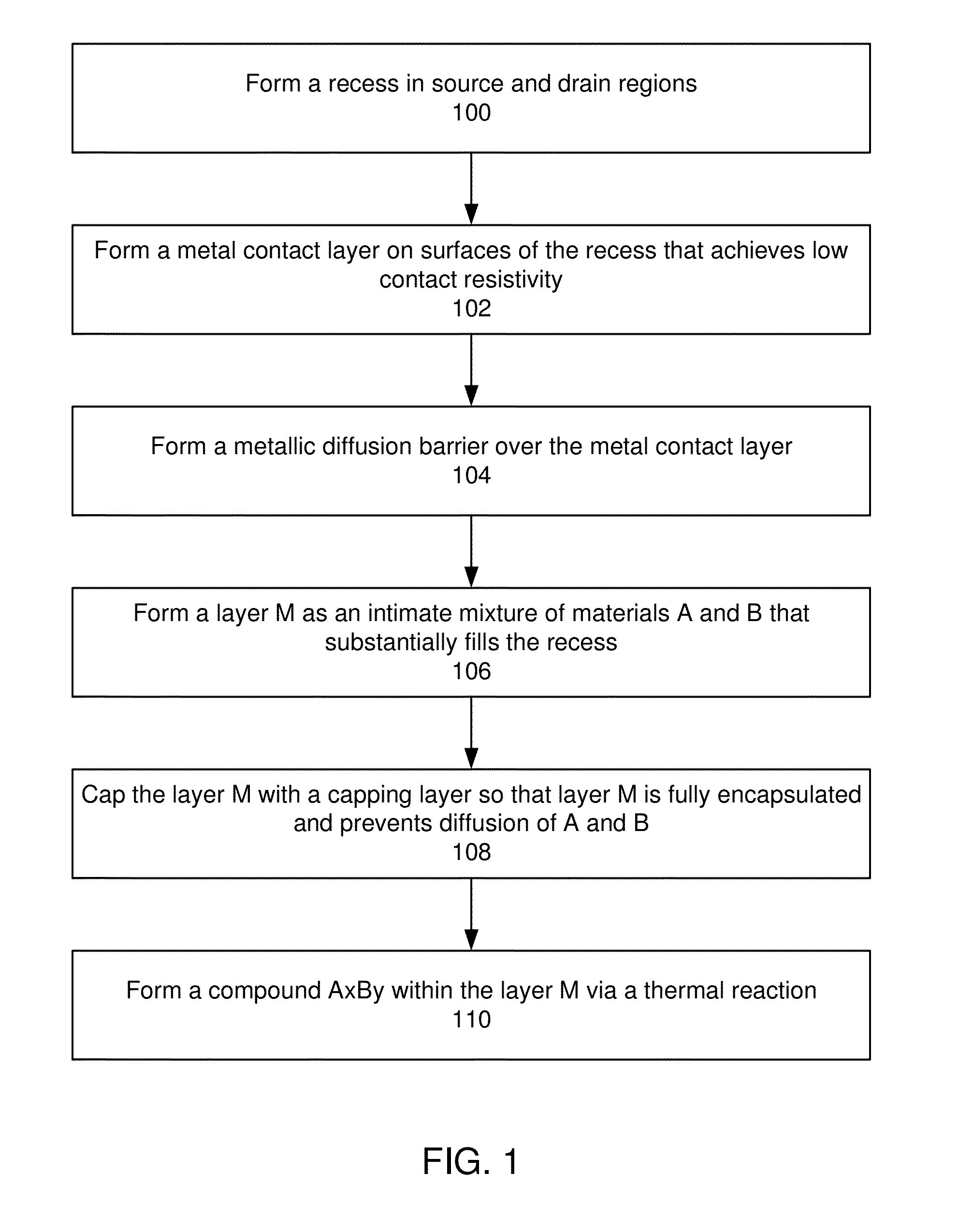
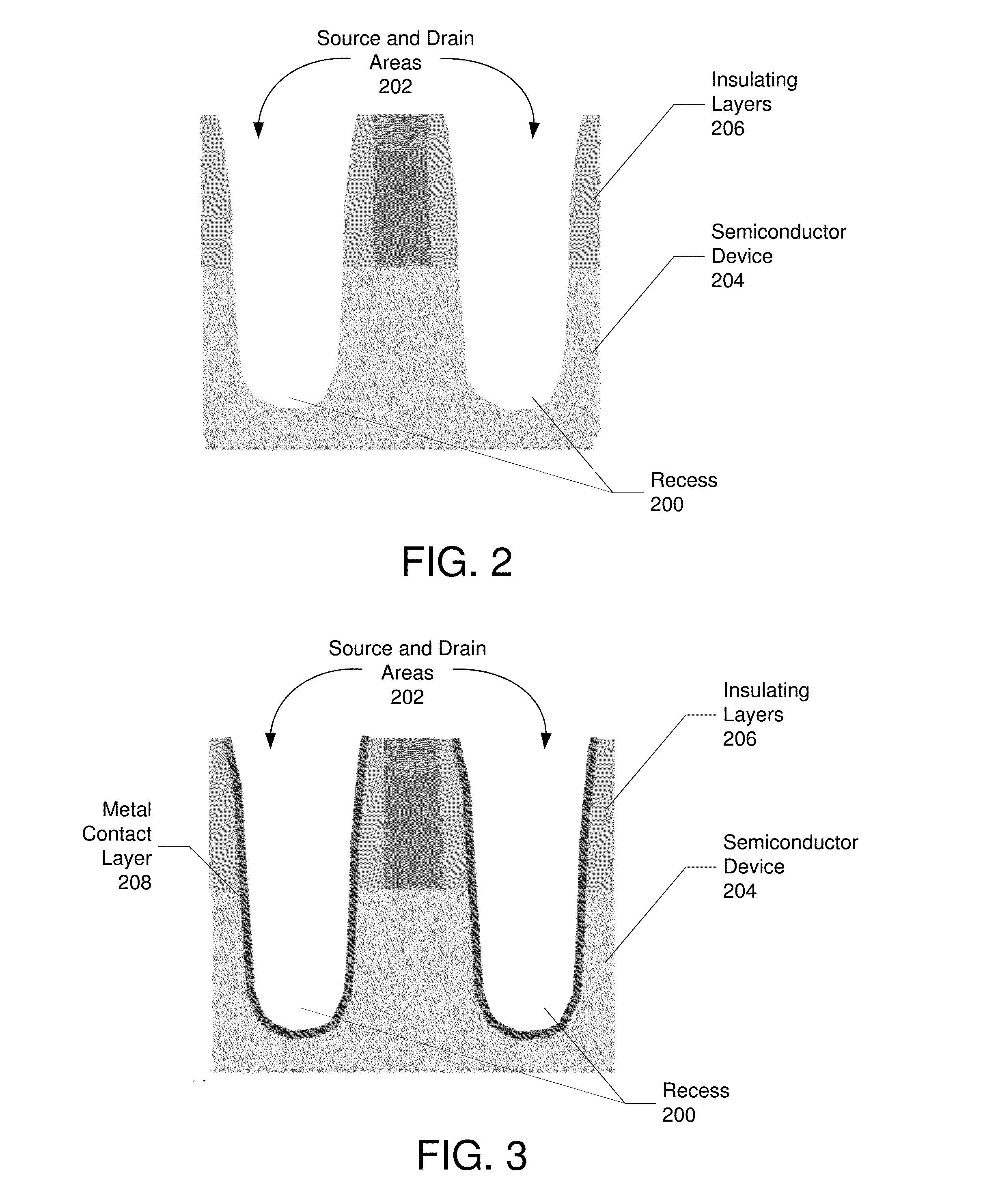
[0014]Reference will now be made in detail to the embodiments of the present general inventive concept, examples of which are illustrated in the accompanying drawings, wherein like reference numerals refer to the like elements throughout. The embodiments are described below in order to explain the present general inventive concept while referring to the figures.

[0015]Advantages and features of the present invention and methods of accomplishing the same may be understood more readily by reference to the following detailed description of embodiments and the accompanying drawings. The present general inventive concept may, however, be embodied in many different forms and should not be construed as being limited to the embodiments set forth herein. Rather, these embodiments are provided so that this disclosure will be thorough and complete and will fully convey the concept of the general inventive concept to those skilled in the art, and the present general inventive concept will only b...


PUM

PropertyMeasurementUnit
thicknessaaaaaaaaaa
thicknessesaaaaaaaaaa
thicknessaaaaaaaaaa

Abstract

Exemplary embodiments provide methods and systems for fabricating a metal source-drain stressor in a MOS device channel having improved tensile stress. Aspects of exemplary embodiment include forming a recess in source and drain areas; forming a metal contact layer on surfaces of the recess that achieves low contact resistivity; forming a metallic diffusion barrier over the metal contact layer; forming a layer M as an intimate mixture of materials A and B that substantially fills the recess; capping the layer M with a capping layer so that layer M is fully encapsulated and the capping layer prevents diffusion of A and B; and forming a compound AxBy within the layer M via a thermal reaction resulting in a reacted layer M comprising the metal source-drain stressor.

Description

CROSS-REFERENCE TO RELATED APPLICATIONS[0001]This application claims the benefit of priority of provisional Patent Application Ser. No. 62 / 077,864 filed on Nov. 10, 2014, is assigned to the assignee of the present application and herein incorporated by reference.BACKGROUND[0002]It is known that silicides in source and / or drain regions can induce strain in channels of metal-oxide-semiconductor field-effect transistor (MOSFET) devices. A silicide in the source / drain (SD) is typically a result of the reaction of a metal layer with SD / channel materials of the semiconductor device. Studies of nickel (Ni), cobalt (Co) and titanium (Ti) silicides used in source and drains for silicon (Si) CMOS technologies, show that the resulting strains induced by silicides on the channel are typically tensile, and originate mostly from the difference in thermal expansion coefficients between the silicide and the substrate / channel material.[0003]Typically, the silicide formation does not result by itself...

Claims


Application Information

Patent Timeline
Patent Type & Authority Applications(United States)
IPC IPC(8): H01L29/78H01L21/768
CPCH01L29/7845H01L21/76883H01L21/7685H01L21/76895H01L29/66636H01L29/66643H01L29/7848H01L21/76897H01L21/28518H01L21/28568H01L21/743H01L21/76843H01L21/76855
Inventor KITTL, JORGE A.HEGDE, GANESHRODDER, MARK S.
Owner SAMSUNG ELECTRONICS CO LTD
Why Eureka
Try Eureka