

Method for manufacturing display panel
a technology of display panel and thin film transistor, which is applied in the direction of instruments, semiconductor devices, electrical apparatus, etc., can solve the problems of affecting the reliability of device operation, the threshold voltage of thin film transistor to shift negatively, etc., and achieve the effect of improving reliability
- Summary
- Abstract
- Description
- Claims
- Application Information
AI Technical Summary
Benefits of technology
Problems solved by technology
Method used
Image

Examples
embodiment
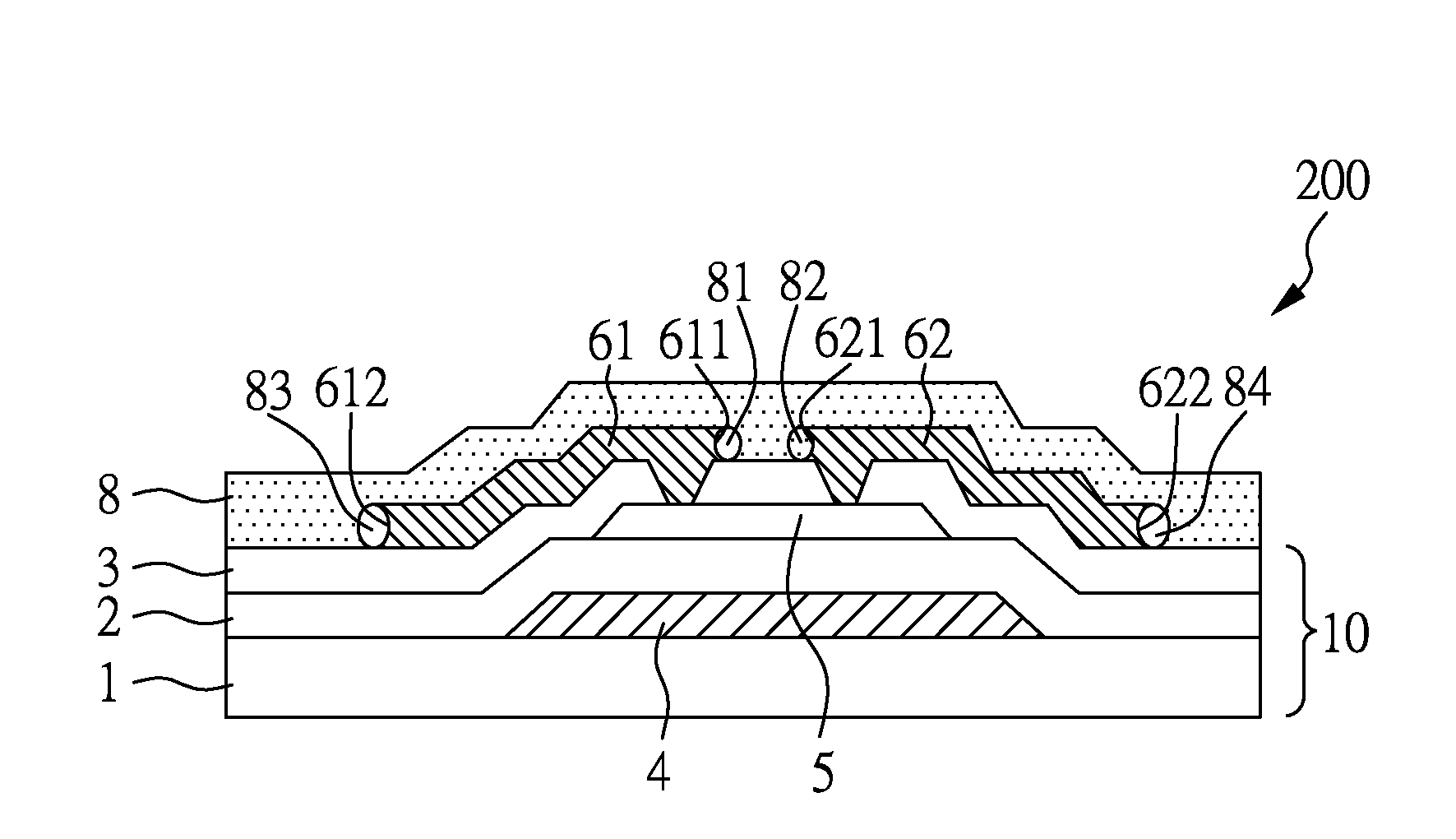
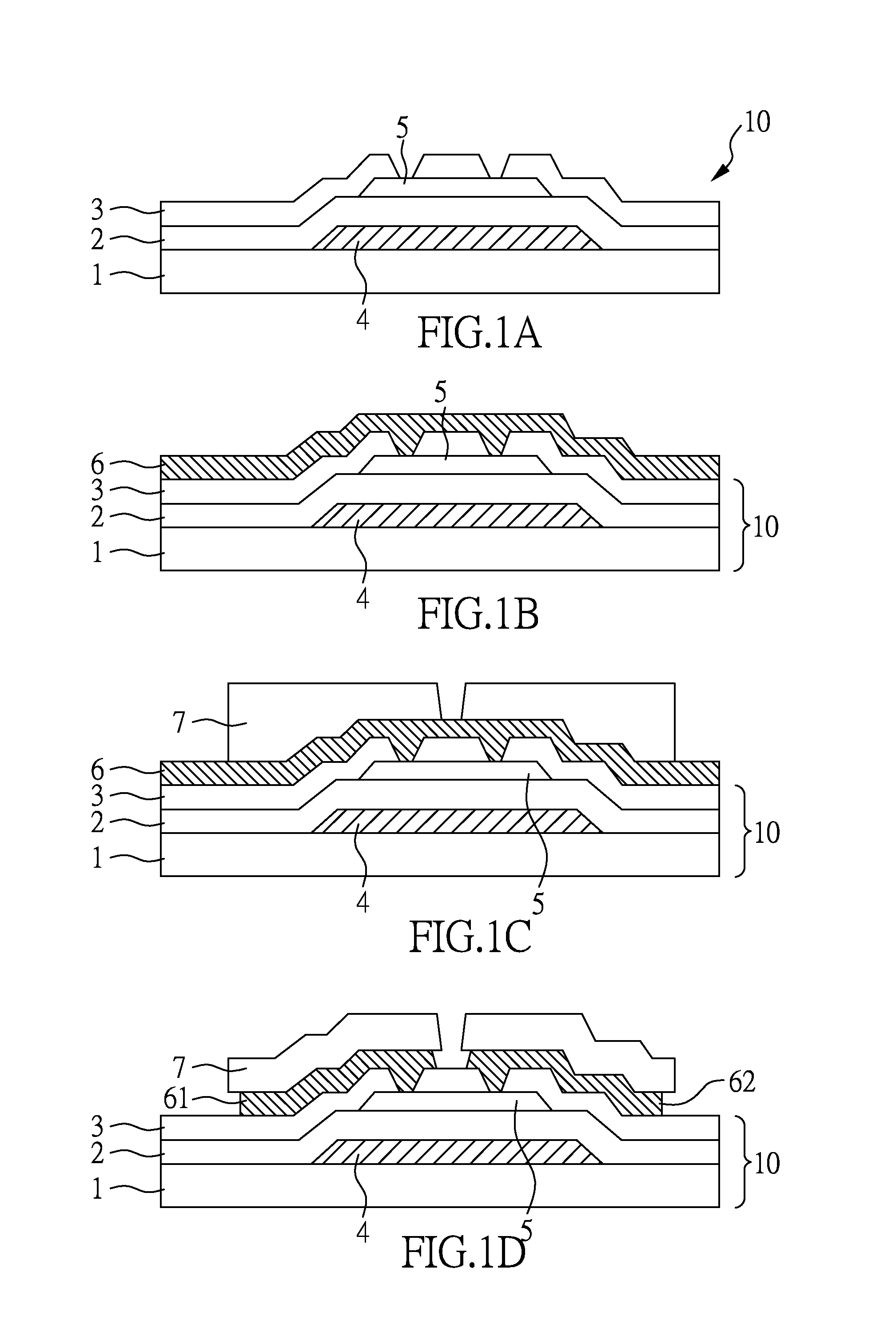
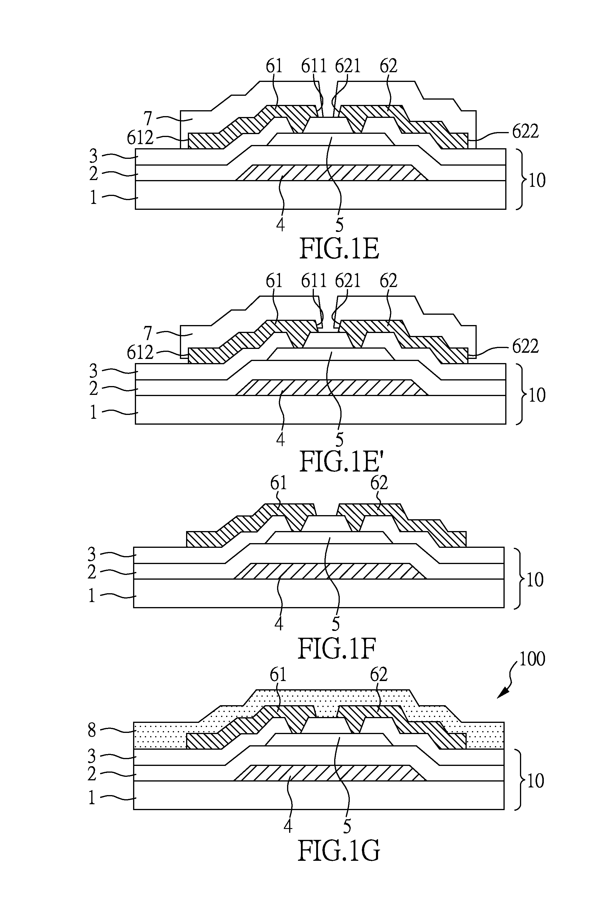
[0025]With reference to FIG. 1A to FIG. 1G, there is shown a schematic diagram of the method for manufacturing a display panel of the present disclosure.
[0026]First of all, as shown in FIG. 1A, there is provided a substrate 1, a first insulating layer 2 and a second insulating layer 3, which are sequentially disposed on the substrate 1; a gate electrode 4 disposed on the substrate 1 and locating between the first insulating layer 2 and the substrate 1; and an oxide semiconductor layer 5 disposed on the substrate 1 and locating between the first insulating layer 2 and the second insulating layer 3; wherein the gate electrode 4 corresponds to the oxide semiconductor layer 5.
[0027]Further, as shown in FIG. 1B, a metal layer 6 is formed on the oxide semiconductor layer 5. Herein, the metal layer 6 having a single-layer or a multi-layer structure may be formed by various deposition methods, such as electroplating, electroless plating, evaporation, sputtering, or combinations thereof. In ...
PUM
| Property | Measurement | Unit |
|---|---|---|
| pH | aaaaa | aaaaa |
| pH | aaaaa | aaaaa |
| pH | aaaaa | aaaaa |
Abstract
Description
Claims
Application Information