Surface Enhanced Raman Spectroscopy Resonator Structures And Methods Of Making Same
- Summary
- Abstract
- Description
- Claims
- Application Information
AI Technical Summary
Benefits of technology
Problems solved by technology
Method used
Image

Examples
first embodiment
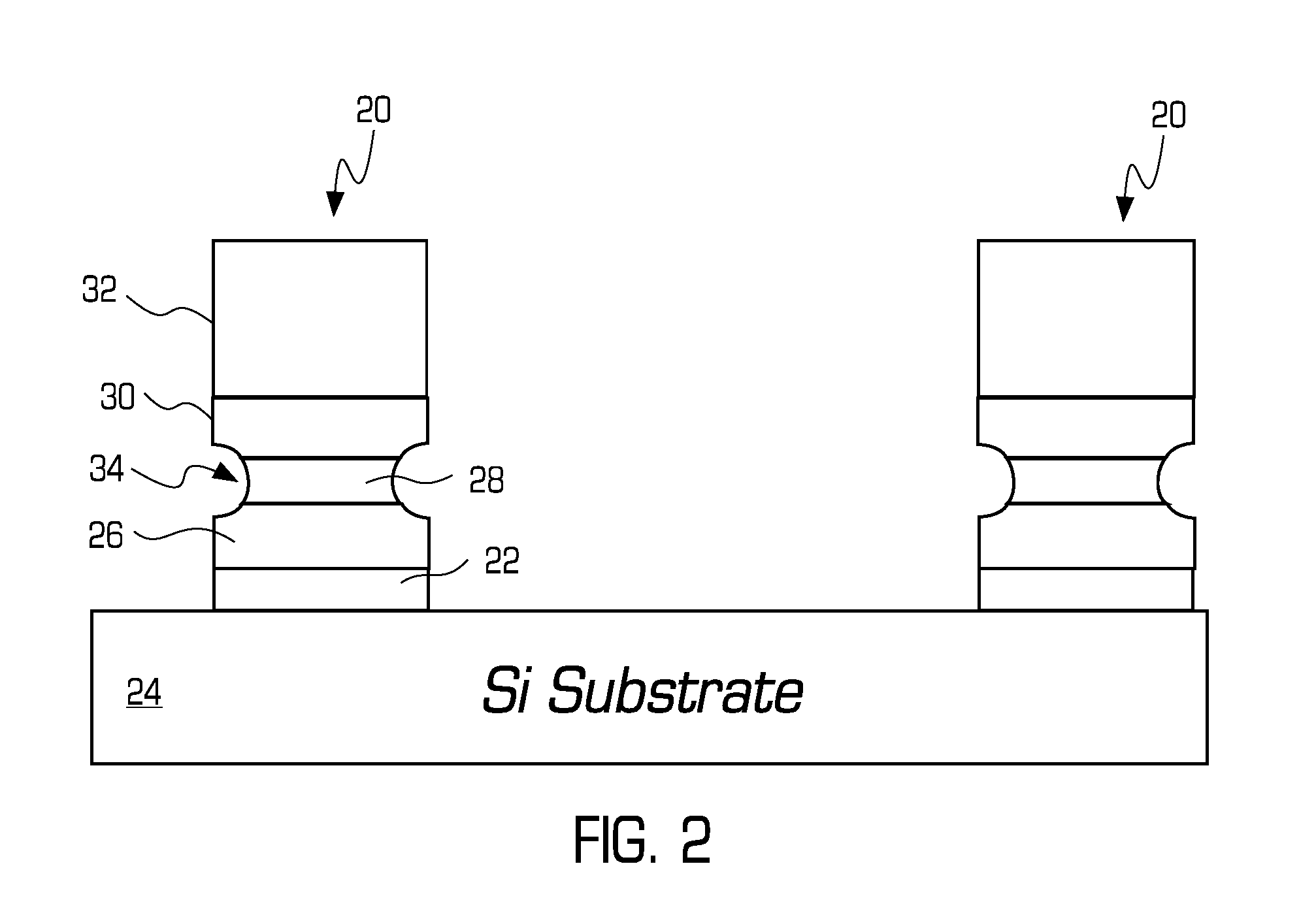
[0017]FIG. 2 illustrates an NPR structure 20 according to a first embodiment of the present invention. NPR structure is fabricated using a photolithographic process that begins by forming a first dielectric layer 22 (e.g. silicon dioxide—SiO2) over a substrate 24 (e.g. Si), followed by forming a first metal layer 26 (e.g. gold or silver) over the first dielectric layer 22, followed by forming a second dielectric layer 28 (e.g. silicon dioxide) over the first metal layer 26, followed by forming a second metal layer 30 (e.g. gold or silver) over the second dielectric layer 28. The metal layers 26 and 30 can be formed by PVD (physical vapor deposition) or ALD (atomic layer deposition). The dielectric layers 22 and 28 can be formed by CVD (chemical vapor deposition) or ALD. The first dielectric layer 22 could instead be formed by thermal oxidation. Photo resist 32 is formed over the second metal layer 30, and patterned using conventional photolithographic masking techniques by selective...
second embodiment
[0020]FIGS. 6-8 illustrate the photolithographic process used to form the NPR structure 44 according to a second embodiment. The process begins by performing a pre-oxidation clean on the substrate 24, followed by forming a first dielectric layer 46 (e.g. silicon dioxide—SiO2) over substrate 24 (e.g. Si), for example by thermal oxidation (e.g. 1 μm thick). This is followed by forming a sacrificial layer 48 over the structure (e.g. polymer that is 0.2 μm to 0.3 μm thick). A BARC layer 50 (Bottom Anti-Reflective Coating, e.g. carbon or inorganic material) is formed over the polymer layer 48. Photo resist 52 is formed over the BARC layer 50, and patterned with holes 54 of approximately 50 nm-250 nm in size (patterning includes photolithograph exposure and photo resist etch). BARC and polymer etches are used to extend the holes 54 down to the first dielectric layer 46. The resulting structure is shown in FIG. 6.
[0021]The photo resist 52 and BARC layer 50 are then removed, and a first lay...
third embodiment
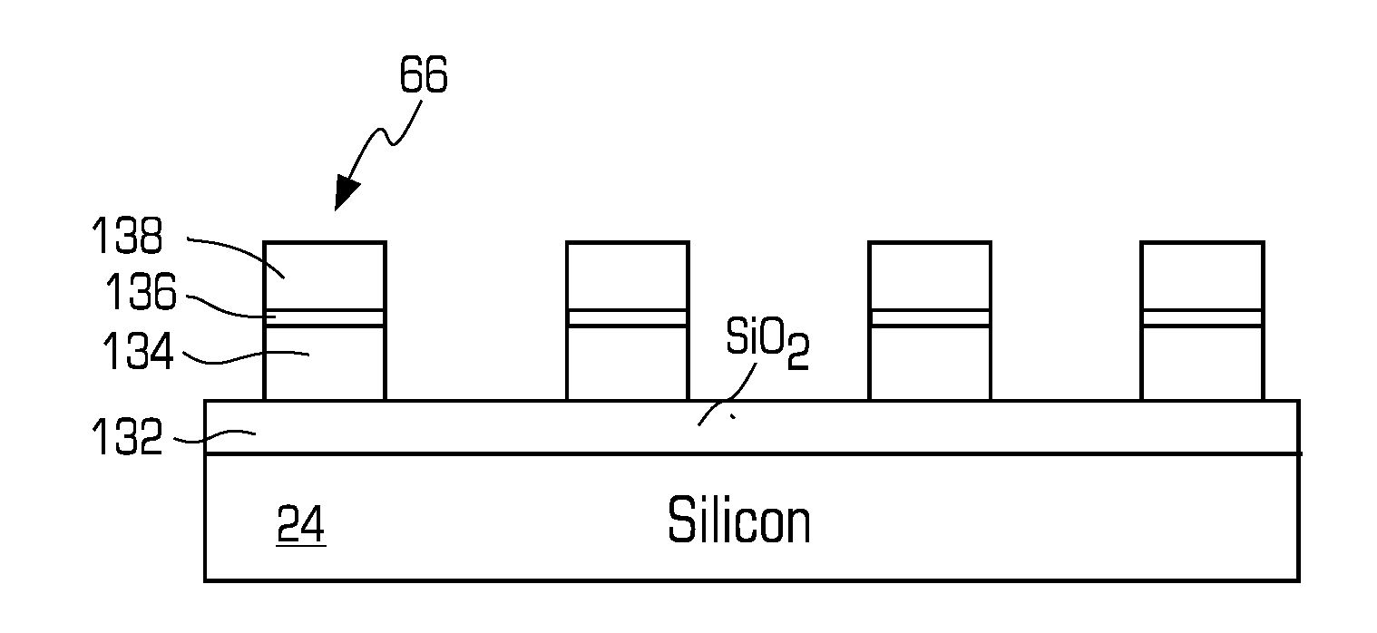
[0024]FIGS. 9A-12A and 9B-12B illustrate the photolithographic process used to form the NPR structure 66 according to a third embodiment. The process begins by performing a pre-oxidation clean of substrate 24, following by forming a first dielectric layer 68 (e.g. silicon dioxide—SiO2) over substrate 24 (e.g. Si), for example by thermal oxidation (e.g. 1 μm). This is followed by forming a sacrificial layer 70 over the structure (e.g. polymer that is 50 nm-10 μm thick). A BARC layer 72 is formed over the polymer 70. Photo resist 74 is formed over the BARC layer 72, and patterned with oval shaped cavities 76, as illustrated in FIGS. 9A and 9B (patterning includes photolithograph exposure and resist etch).
[0025]BARC and polymer etches are used to extend the cavities 76 defined by the photo resist down through the BARC and polymer layers 72, 70 (i.e. down to and exposing the first dielectric layer 68). The photo resist 74 is then removed. A second photo resist is formed over the BARC la...
PUM
 Abstract
Description
Claims
Application Information
 - R&D Engineer
- R&D Manager
- IP Professional
- Industry Leading Data Capabilities
- Powerful AI technology
- Patent DNA Extraction
Browse by: Latest US Patents, China's latest patents, Technical Efficacy Thesaurus, Application Domain, Technology Topic.
© 2024 PatSnap. All rights reserved.Legal|Privacy policy|Modern Slavery Act Transparency Statement|Sitemap