Semiconductor device and method for manufacturing semiconductor device

Inactive Publication Date: 2016-05-26
TOYOTA JIDOSHA KK
View PDF0 Cites 8 Cited by
  • Summary
  • Abstract
  • Description
  • Claims
  • Application Information

AI Technical Summary

Benefits of technology

[0009]This method makes it possible to manufac...

Problems solved by technology

The occurrence of a punch-through generates a leak current, thus presenting a problem.
Further, tuning off this semiconducto...

Method used


Image

  • Semiconductor device and method for manufacturing semiconductor device
  • Semiconductor device and method for manufacturing semiconductor device
  • Semiconductor device and method for manufacturing semiconductor device

Examples


embodiment 1

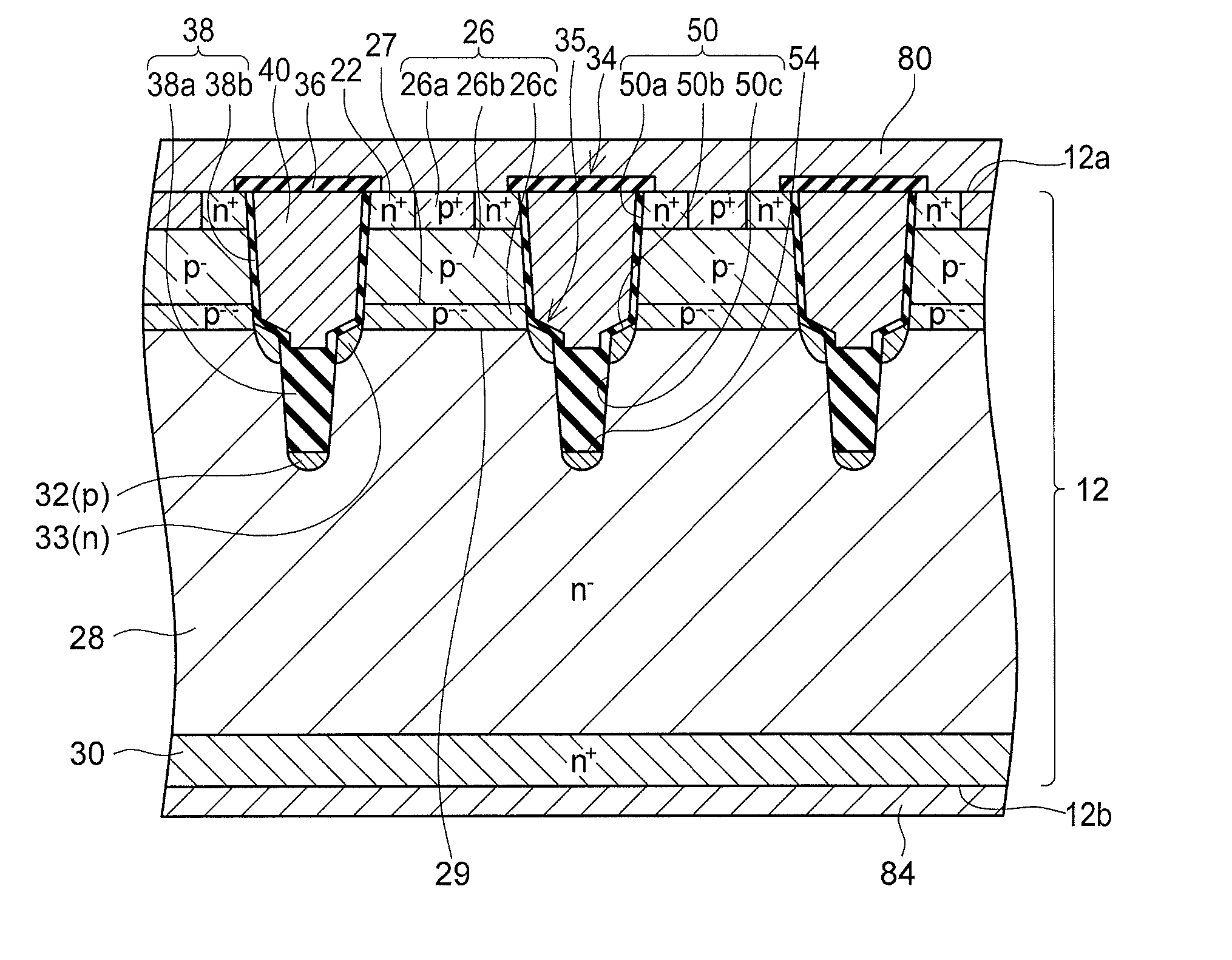
[0024]As shown in FIG. 1, a semiconductor device 10 according to Embodiment 1 includes a semiconductor substrate 12 and electrodes, insulating layers, and the like located on a front surface 12a and / or a back surface 12b of the semiconductor substrate 12. The semiconductor substrate 12 is made of 4H—SiC.

[0025]A source electrode 80 is located on the front surface 12a of the semiconductor substrate 12. A drain electrode 84 is located on the back surface 12b of the semiconductor substrate 12. The drain electrode 84 covers substantially a whole area of the back surface 12b.

[0026]Each trench 34 has a side surface 50. A step 35 is formed in the side surface 50 of the each trench 34. The side surface 50 of the each trench 34 includes an upper side surface 50a located on an upper side with respect to the step 35, a step surface 50b which is a surface of the step 35, and a lower side surface 50c located on a lower side with respect to the step 35. The step surface 50b of the step 35 slopes ...

embodiment 2

[0050]As shown in FIG. 9, a semiconductor device according to Embodiment 2 has steps 35 located at a level lower than a level of the boundary 27 between the upper region 26b and the lower region 26c. The steps 35 are located on an upper side with respect to the p-n junction 29 at a boundary between the lower region 26c and the drift region 28. The other components of the semiconductor device of Embodiment 2 are identical to those of the semiconductor device 10 of Embodiment 1. Also in the semiconductor device according to Embodiment 2, the side regions 33 protrude toward an upper side with respect to the drift region 28. This makes it possible to achieve compatibility between the channel length and the punch-through voltage. Further, by taking a longer etching time to form the trenches 34 than in Embodiment 1, the steps 35 can be located at the level lower than the level of the boundary 27 between the upper region 26b and the lower region 26c as in Embodiment 2.

embodiment 3

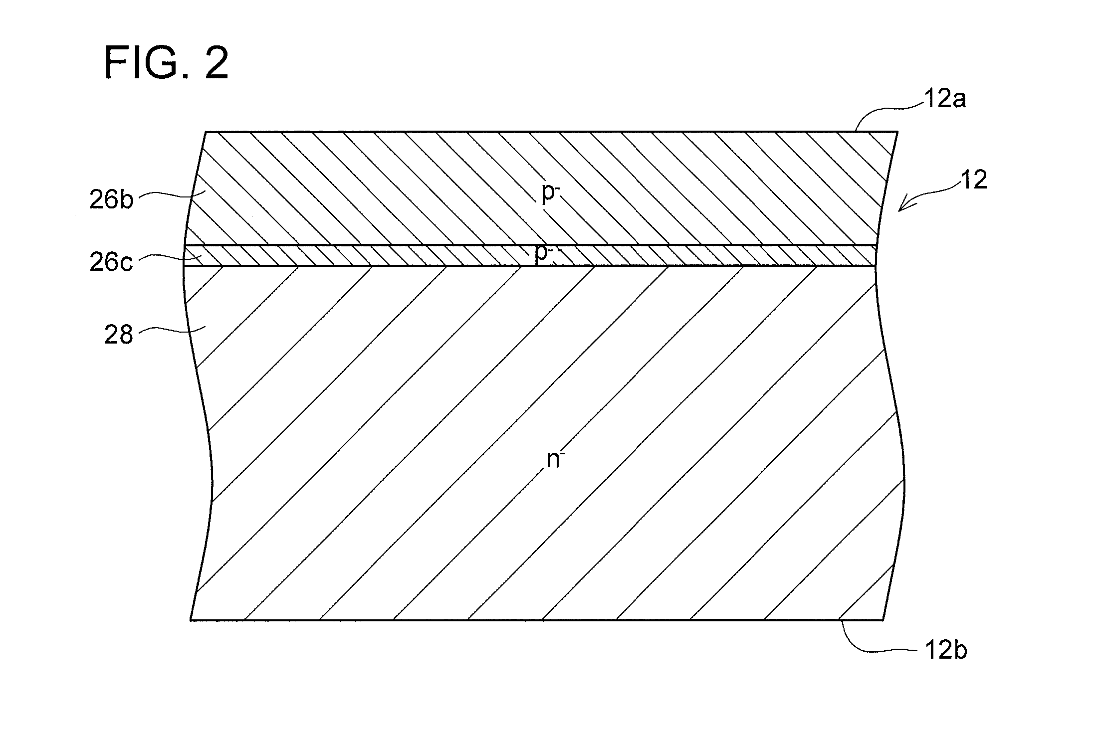
[0051]As shown in FIG. 10, a semiconductor device according to Embodiment 3 has steps 35 that do not slope. That is, the steps 35 are formed substantially parallel to the surface 12a of the semiconductor substrate 12. Further, in the semiconductor device according to Embodiment 3, the body region 26, on a lower side with respect to the high-concentration region 26a, includes only a low-concentration region 26d. That is, whereas the body region 26 includes the upper region 26b and the lower region 26c on the lower side with respect to the high-concentration region 26a in Embodiment 1, a p-type impurity concentration in a portion (i.e. the low-concentration region 26d) of the body region 26 that is located on the lower side with respect to the high-concentration region 26a is substantially uniform. The p-type impurity concentration of the low-concentration region 26d is lower than that of the high-concentration region 26a. Also in the semiconductor device according to Embodiment 3, th...


PUM


Abstract

A semiconductor device includes a semiconductor substrate including a trench, a gate insulating layer, and a gate electrode. A step is arranged in a side surface of the trench. The semiconductor substrate includes first and second regions, a body region, and a side region. The body region extends from a position being in contact with the first region to a position located on the lower side with respect to the step. The body region is in contact with the gate insulating layer at a portion of the upper side surface located on a lower side with respect to the first region. The second region is located on a lower side of the body region and in contact with the gate insulating layer at the lower side surface. The side region is in contact with the gate insulating layer at the step surface and connected to the second region.

Description

CROSS-REFERENCE TO RELATED APPLICATION[0001]This application claims priority to Japanese Patent Application No. 2014-236545 filed on Nov. 21, 2014, the contents of which are hereby incorporated by reference into the present application.TECHNICAL FIELD[0002]A technology disclosed herein relates to a semiconductor device having a gate electrode disposed in a trench.DESCRIPTION OF RELATED ART[0003]Japanese Patent Application Publication No. 2006-128507 A discloses a MOSFET having a gate electrode disposed in a trench. This MOSFET includes a semiconductor substrate in which an n-type source region, a p-type body region, and an n-type drift region are provided. That is, this MOSFET is of an n-channel type. Application of a predetermined potential to the gate electrode causes a portion of the body region that is adjacent to a gate insulating layer to be inverted into n-type, and a current flows through the region (i.e. a channel) thus inverted into n-type.BRIEF SUMMARY[0004]In the MOSFET ...

Claims


Application Information

Patent Timeline
IPC IPC(8): H01L29/78H01L29/06H01L21/28H01L21/225H01L21/306H01L29/66H01L29/10
CPCH01L29/7813H01L29/66734H01L29/0696H01L21/28008H01L29/1045H01L21/2253H01L21/30604H01L29/1095H01L29/0603H01L29/1033H01L29/66492H01L29/7834H01L21/3065H01L21/3083H01L29/42368H01L29/42376H01L29/0623H01L29/0878
Inventor TAKAYA, HIDEFUMIKUTSUKI, KATSUHIROAOI, SACHIKOMIYAHARA, SHINICHIRO
Owner TOYOTA JIDOSHA KK
Why Eureka
Try Eureka