Switched power stage with integrated passive components
Inactive Publication Date: 2016-06-02
CHAOYANG SEMICON JIANGYIN TECH CO LTD
View PDF6 Cites 10 Cited by
Summary
Abstract
Description
Claims
Application Information
AI Technical Summary
This helps you quickly interpret patents by identifying the three key elements:
Problems solved by technology
Method used
Benefits of technology
Benefits of technology
The invention is about a structure that uses micro-bumps and RDL metallization to create a desired magnetic field path in a switching voltageregulator. This structure is designed to maximize and minimize the inductance on the switches of the regulator. The size and current capability of the micro-bumps are chosen to match the inductor core area, magnetic fieldpath length, and the number of turns that can be constructed to achieve the desired inductance with a high L / R ratio. This structure can be used in a multiphase buck converter or other types of converters with coupling inductors. The technical effect of this invention is to improve the performance and efficiency of switching voltage regulators.
Problems solved by technology
This generally results in a significant parasitic inductance which has become a significant limiting factor in the performance of the mobile devices as higher frequencies and higher currents generate local transient effects, which are also referred to as droops due to fast changes in the load currents.
One of the biggest challenges, however, in implementing an eVR is to manufacture inductors with high inductance to resistance value (L / R: inductance [nH] per resistance [mohms]) with small form factor (current rating per square millimeter).
Method used
Image
Click on the blue label to locate the original text in one second.
Reading with bidirectional positioning of images and text.
Examples
example 1
With a Structure as Shown in FIG. 6
[0051]Process node: 180 nm
[0052]Current rating: 1 A per bump
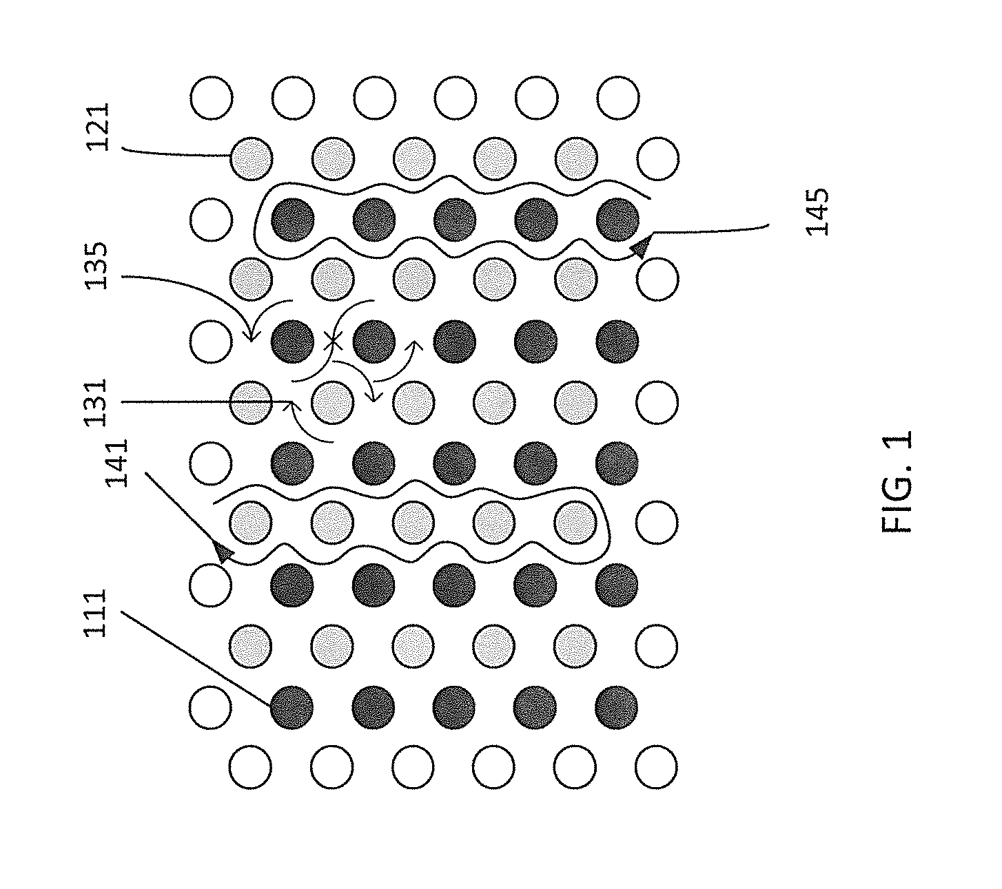
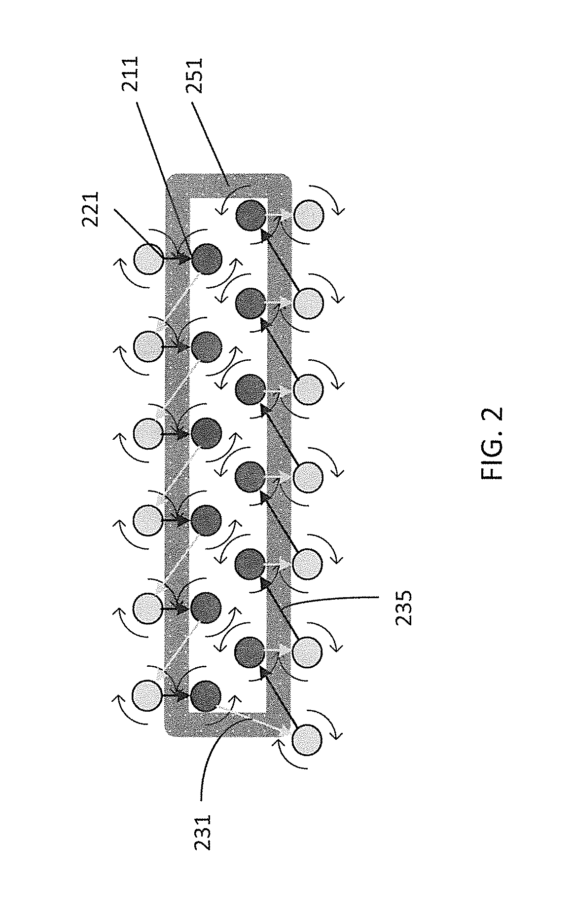
[0053]Magnetic Path Length / Core Area: 1.8 mm / (70 um×50 um)×3 (3 “cores” as shown in FIG. 6)
[0057]Note that the core area shown in the figures, bounded by magnetic path lines, can be filled with magnetic material and the 1 nH would increase proportional to the relative permeability of the material. Ideally the VDD / GND area would not be filled with the magnetic material and will stay more or less<50 pH.
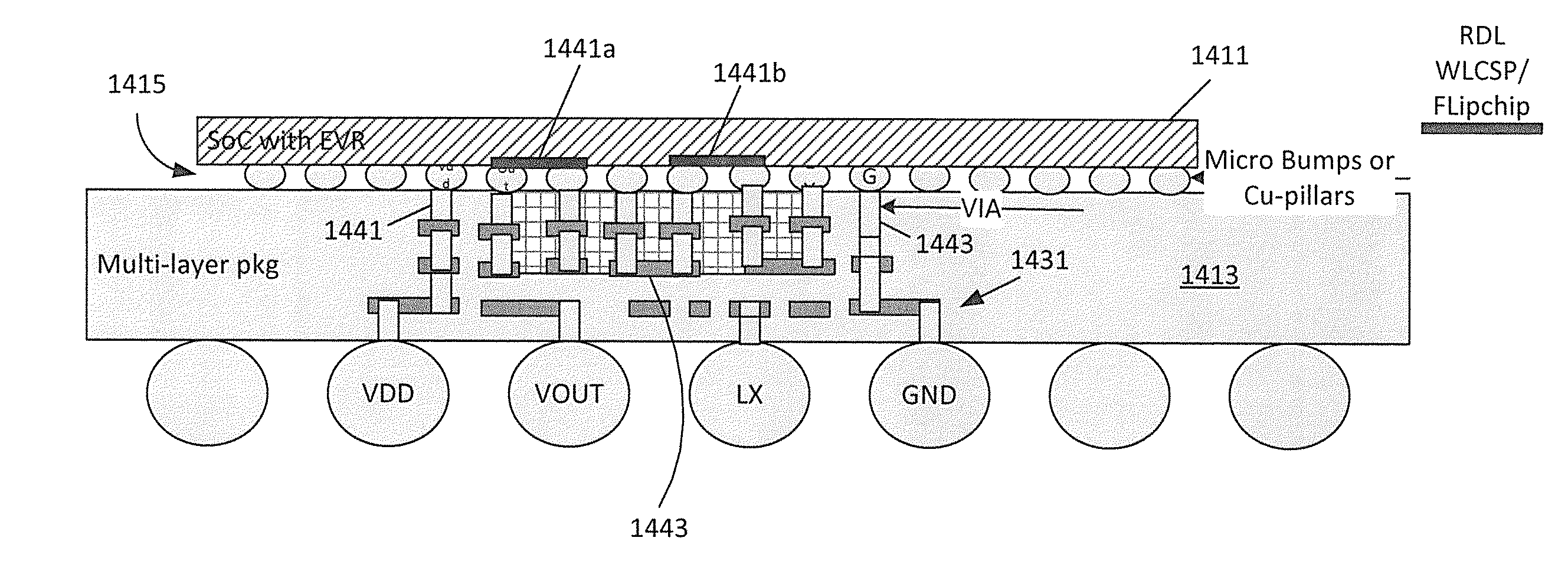
[0074]FIG. 12 shows a typical flip chip multi-layer substrate package. In FIG. 12 the RDLs and in between vias are used for routing. In FIG. 12, an SOC (including an embedded voltage regulator) 1211 is coupled to signal paths in a multi-layer substrate 1213 by way of micro-bumps 1215. Vias, for example via 1217, and RDLs, for example RDL 1219, electrically couple various of the micro-bumps to various solder balls, for example a ground GND solder ball 1221. The solder balls in turn electrically couple the signal paths of the multi-layer substrate to a printed circuit board (PCB) 1223. As shown in FIG. 12, the PCB additionally inc...
PUM
Abstract
A scalable switching regulator architecture may include an integrated inductor. The integrated inductor may include vias or pillars in a multi-layer substrate, with selected vias coupled at one end by a redistribution layer of the multi-layer substrate and, variously, coupled at another end by a metal layer of a siliconintegrated circuitchip or by a further redistribution layer of the multi-layer substrate. The vias may be coupled to the siliconintegrated circuitchip by micro-balls, with the vias and micro-balls arranged in arrays.
Description
CROSS REFERENCE TO RELATED APPLICATION[0001]This application claims the benefit of the filing date of U.S. Provisional Patent Application No. 62 / 086,081, filed on Dec. 1, 2014, the disclosure of which is incorporated by reference herein.BACKGROUND OF THE INVENTION[0002]A power distribution network (PDN) in a system-on-chip (SoC) used in various mobile device typically includes on-chip metallization layers connecting to a package substrate via micro-bumps or copper pillars. The micro-bumps may be connected to balls of the package by vias and one or more redistribution layers (RDLs) within the package, with the balls of the package coupled to a printed circuit board (PCB). This generally results in a significant parasitic inductance which has become a significant limiting factor in the performance of the mobile devices as higher frequencies and higher currents generate local transient effects, which are also referred to as droops due to fast changes in the load currents.[0003]In order...
Claims
Application Information
Patent Timeline
Application Date:The date an application was filed.
Publication Date:The date a patent or application was officially published.
First Publication Date:The earliest publication date of a patent with the same application number.
Issue Date:Publication date of the patent grant document.
PCT Entry Date:The Entry date of PCT National Phase.
Estimated Expiry Date:The statutory expiry date of a patent right according to the Patent Law, and it is the longest term of protection that the patent right can achieve without the termination of the patent right due to other reasons(Term extension factor has been taken into account ).
Invalid Date:Actual expiry date is based on effective date or publication date of legal transaction data of invalid patent.

