Semiconductor device and fabrication method thereof

a technology of semiconductor devices and semiconductor components, applied in semiconductor devices, semiconductor/solid-state device details, inductances, etc., can solve the problems of poor inductance performance, low quality factor q of existing planar inductor, and low integration level of the fabrication process of the planar inductor with the fabrication process of other semiconductor devices

Active Publication Date: 2016-06-09
SEMICON MFG INT (SHANGHAI) CORP
View PDF12 Cites 4 Cited by
  • Summary
  • Abstract
  • Description
  • Claims
  • Application Information

AI Technical Summary

Problems solved by technology

Specifically, the higher the resistance is, or the higher the parasitic capacitance is, the smaller the quality factor Q is, and the worse the performance of the inductor is.
However, the quality factor Q of the existing planar inductor is subst

Method used


Image

  • Semiconductor device and fabrication method thereof
  • Semiconductor device and fabrication method thereof
  • Semiconductor device and fabrication method thereof

Examples


Embodiment Construction

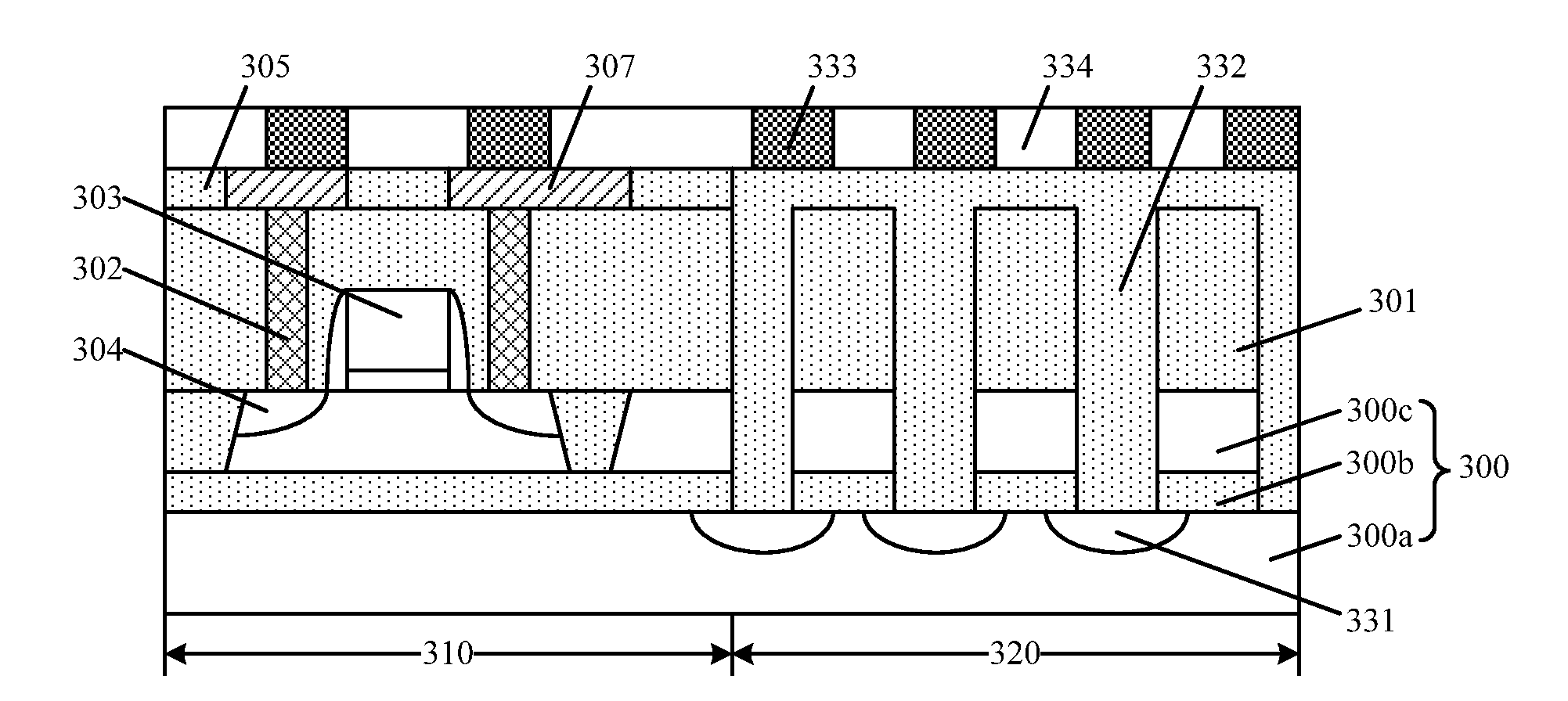
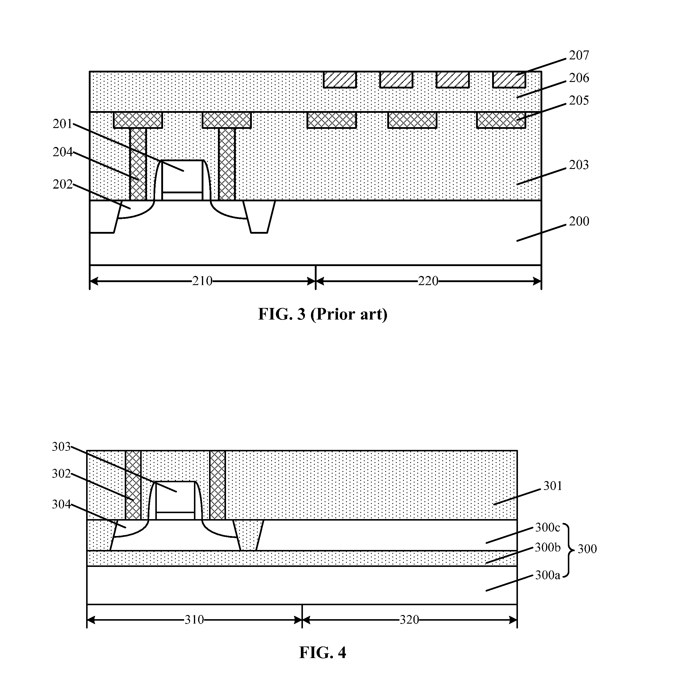
[0016]Reference will now be made in detail to exemplary embodiments of the invention, which are illustrated in the accompanying drawings. Wherever possible, the same reference numbers will be used throughout the drawings to refer to the same or like parts.

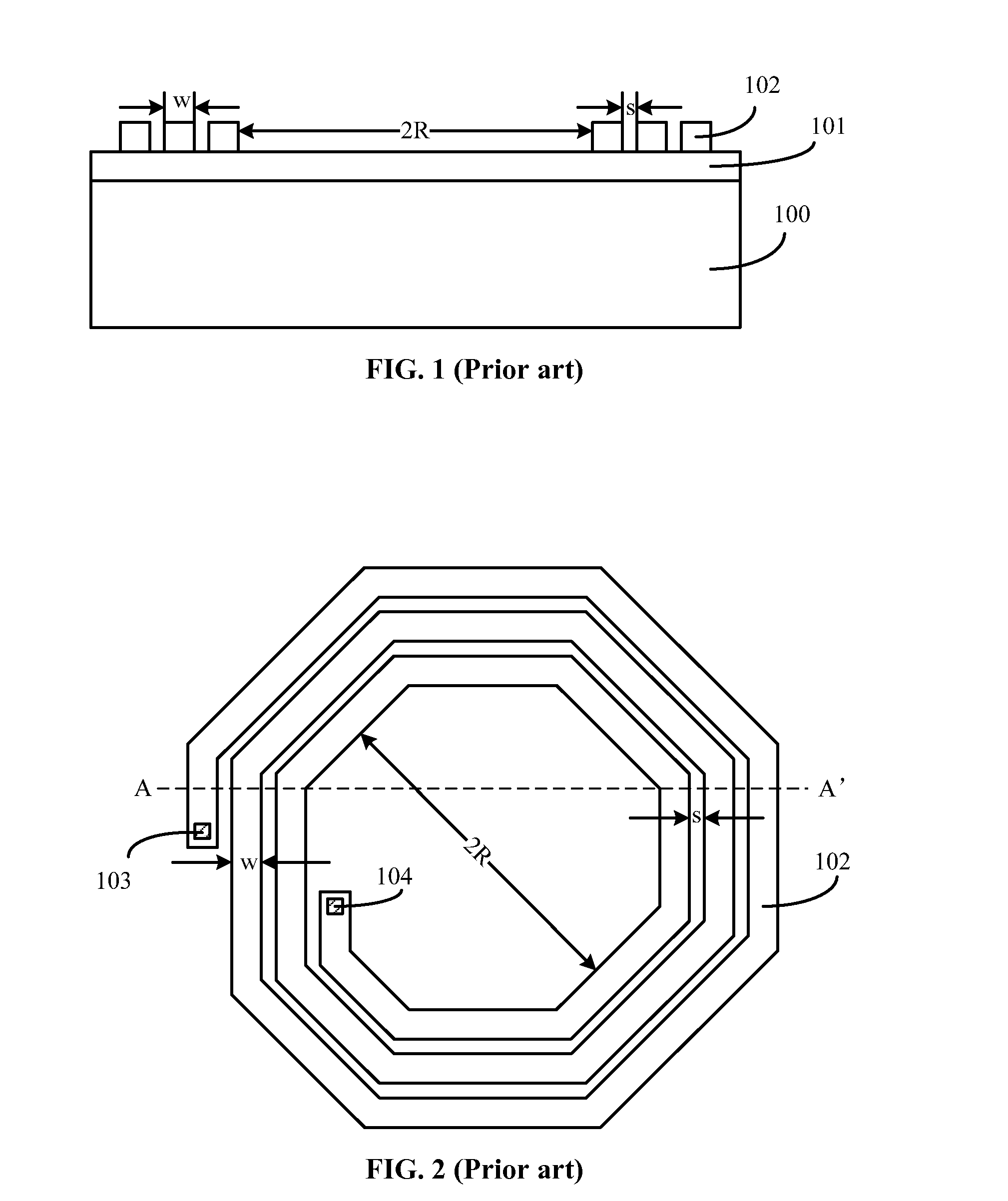
[0017]Referring to FIGS. 1˜2, when the inductor is in operation, an electrical current flows in the planar coil 102, the spiral current may be able to generate an electromagnetic field perpendicular to the surface of the semiconductor substrate 100. According to the Lenz's law, the electromagnetic field penetrating through the semiconductor substrate 200 may induce a current, and the direction of the induced current may be opposite to the current in the planar coil 102. The induced current may also be able to generate a magnetic field perpendicular to the planar coil 102. Because the direction of the inducted current may be opposite to the direction of the current in the planar coil 102, the strength of the magnetic field of the in...


PUM


Abstract

A method for forming a semiconductor device includes, sequentially, providing a substrate having a first region and a second region; forming a first dielectric layer on the substrate; forming a second dielectric layer having a plurality of first openings exposing portions of a top surface of the first dielectric layer; forming a first conductive layer in the first openings; etching the second dielectric layer and the first dielectric layer in the second region until the substrate is exposed to form a plurality of second openings; forming passivation regions in portions of the substrate exposed by the second openings; exposing the surface of the first dielectric layer in the second region; forming a third dielectric layer on the surface of the first dielectric layer and in the second openings; and forming a second conductive layer, a portion of which is configured as an inductor, over the third dielectric layer.

Description

CROSS-REFERENCES TO RELATED APPLICATIONS[0001]This application claims the priority of Chinese patent application No. 201410734496.5, filed on Dec. 4, 2014, the entirety of which is incorporated herein by reference.FIELD OF THE INVENTION[0002]The present invention generally relates to the field of semiconductor manufacturing technology and, more particularly, relates to semiconductor devices and fabrication processes thereof.BACKGROUND[0003]In some integrated circuits (ICs), such as the radio frequency front-end modules (RF FEMs), etc., inductors are important electronic devices. The specific parameters of the inductors directly affect the performance of those ICs. In existing technologies, inductors are often planar inductors, such as planar spiral inductors, etc. The planar inductors are formed by winding a metal wire on the surface of a substrate or a dielectric layer. Comparing with conventional coil inductors, the planar inductors have the advantages including low cost, easy int...

Claims


Application Information

Patent Timeline
IPC IPC(8): H01L23/522H01L27/06H01L21/033H01L21/768H01L23/532H01L49/02H01L21/288H01L21/321H01L23/528H01L23/31H01L21/311
CPCH01L23/5227H01L23/53228H01L27/0641H01L27/0617H01L27/0676H01L21/0332H01L21/76802H01L21/76877H01L21/31144H01L23/5226H01L28/10H01L21/7684H01L21/2885H01L21/3212H01L23/528H01L23/3171H01L21/02164H01L21/02271H01L21/3065H01L21/3081H01L21/31116H01L21/76264H01L23/53295H01L2924/0002H01L2924/00
Inventor BAO, XIAOYANGE, HONGTAO
Owner SEMICON MFG INT (SHANGHAI) CORP
Why Eureka
Try Eureka