Semiconductor light emitting element and method for manufacturing the same

Active Publication Date: 2016-06-09
STANLEY ELECTRIC CO LTD +1
View PDF8 Cites 11 Cited by
  • Summary
  • Abstract
  • Description
  • Claims
  • Application Information

AI Technical Summary

Benefits of technology

[0017]According to the present invention, the semiconductor light emittin

Problems solved by technology

However, when the light passes through a boundary between media having different refractive indexes, i.e., an interface between layers or a surface, a certain rate of reflection occurs inevitably.
Therefore, it is generally difficult to efficiently extract the light emitted in the light emitting layer to the outside of the semiconductor light emitting element.
However, it is not easy to form the nanometer-scale recessed and projecting structure on the surface of the semiconductor light emitting element.
In addition, the light extraction efficiency greatly varies depending on the shape of the recessed and projecting structure and the emission wavelength, and thus, the effect is not sufficiently obtained.
As the emission wavelength becomes shorter, the required period of the recessed and projecting structure (e.g., in the case of a projecting structure, a distance between a vertex portion of a projecting structure and a vertex portion of an adjacent projecting structure) becomes shorter, and thus, fabrication of the recessed and projecting structure becomes difficult.
Particularly in a semiconductor light emitting element that emits the light in an ultraviolet or deep ultraviolet wavelength range, it is difficult to fabricate the recesse

Method used


Image

  • Semiconductor light emitting element and method for manufacturing the same
  • Semiconductor light emitting element and method for manufacturing the same
  • Semiconductor light emitting element and method for manufacturing the same

Examples


first embodiment

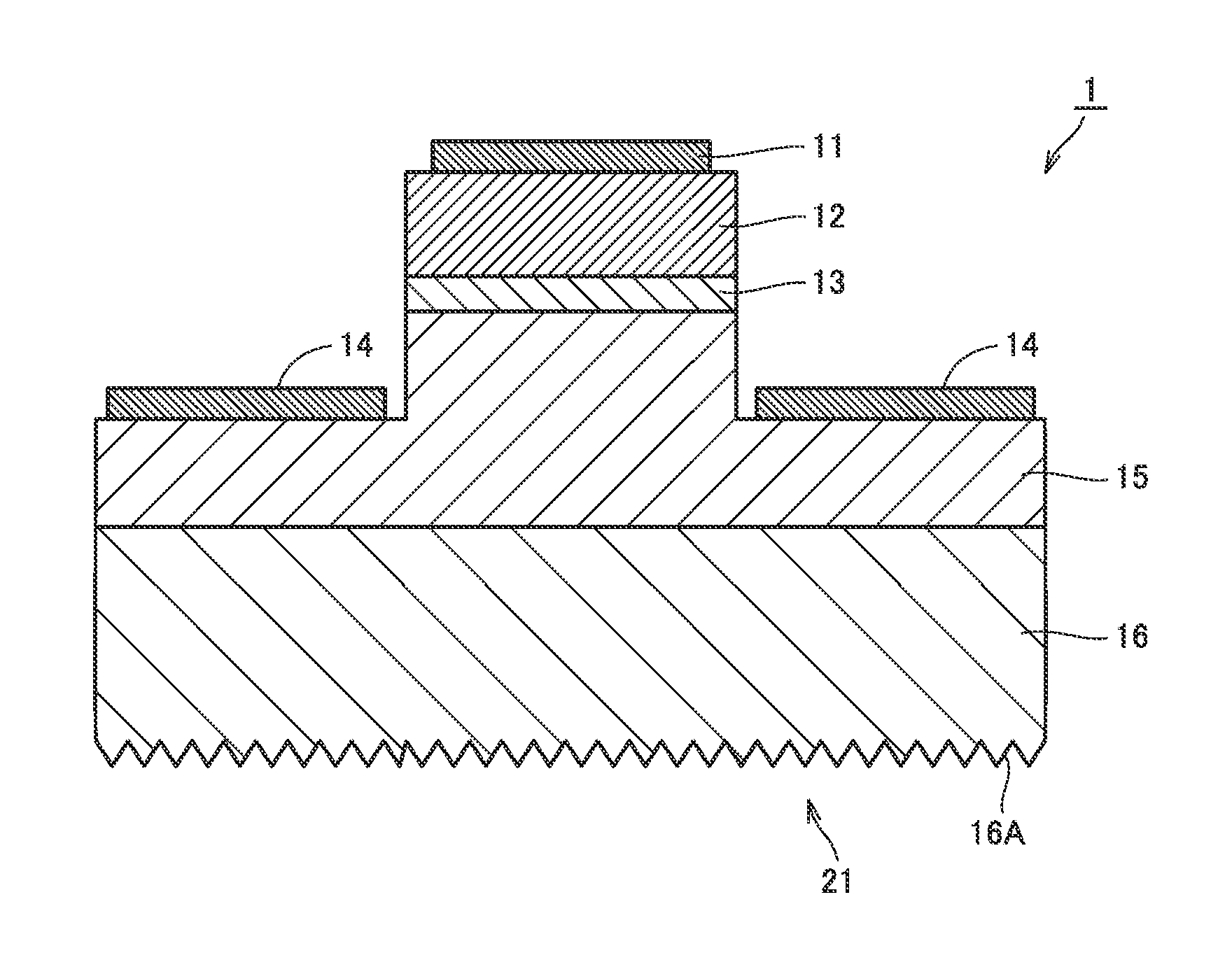
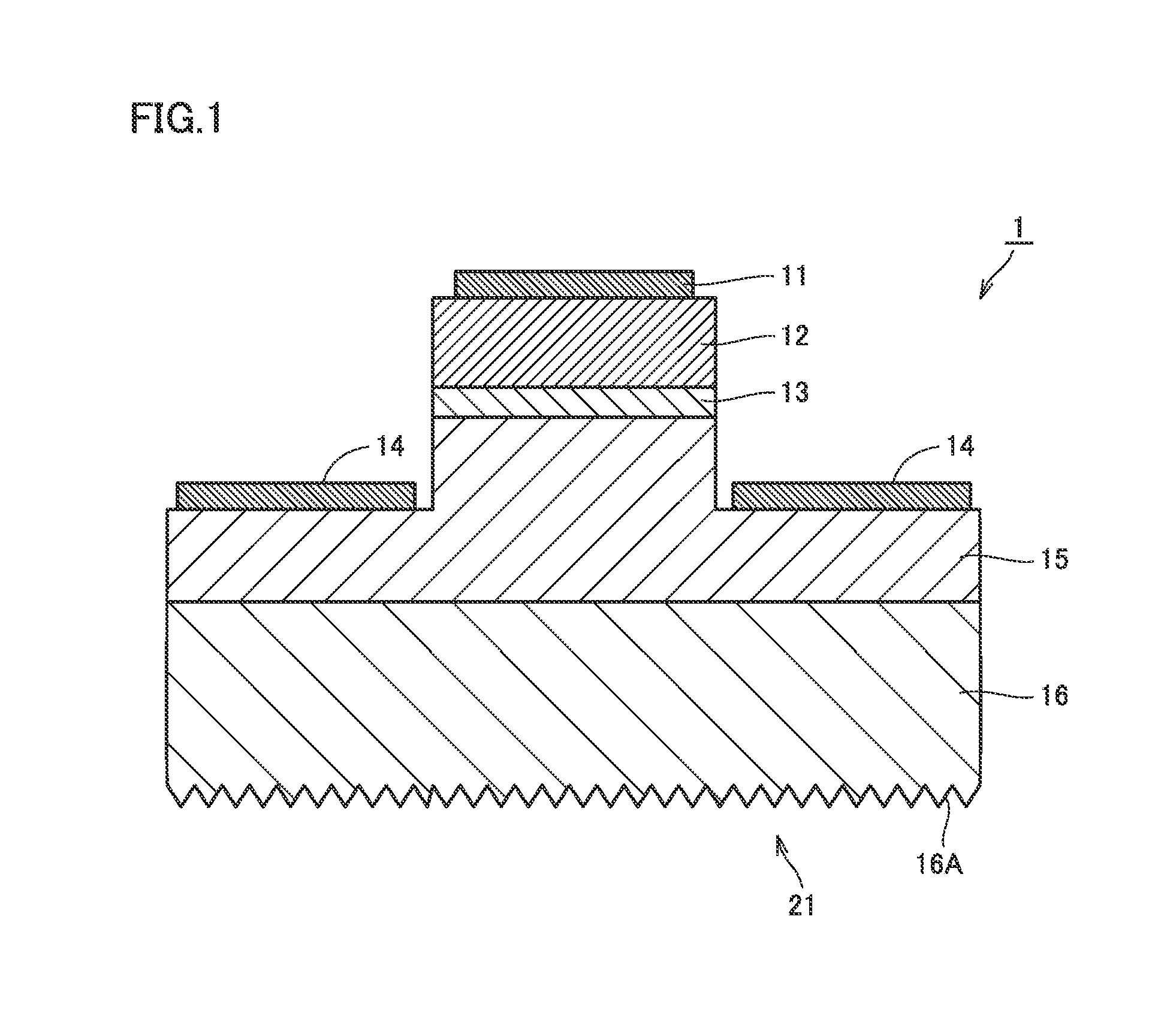
[0069]FIGS. 1 to 3 conceptually show a structure of a semiconductor light emitting element according to a first embodiment of the present invention. Referring to FIGS. 1 to 3, the semiconductor light emitting element mainly includes a substrate 16 made of AlN (aluminum nitride), an n-type semiconductor layer 15, an active layer 13, a p-type semiconductor layer 12, a positive electrode 11, and a negative electrode 14. N-type semiconductor layer 15 is formed on a main surface of substrate 16. A projection is formed on a part of a surface of n-type semiconductor layer 15, and active layer 13 is formed on this projection. P-type semiconductor layer 12 is formed on active layer 13. Positive electrode 11 is formed on p-type semiconductor layer 12. In addition, negative electrode 14 is formed in a region on the surface of n-type semiconductor layer 15 where the aforementioned projection is not formed.

[0070]A wavelength of the light emitted from active layer 13 serving as a light emitting l...

second embodiment

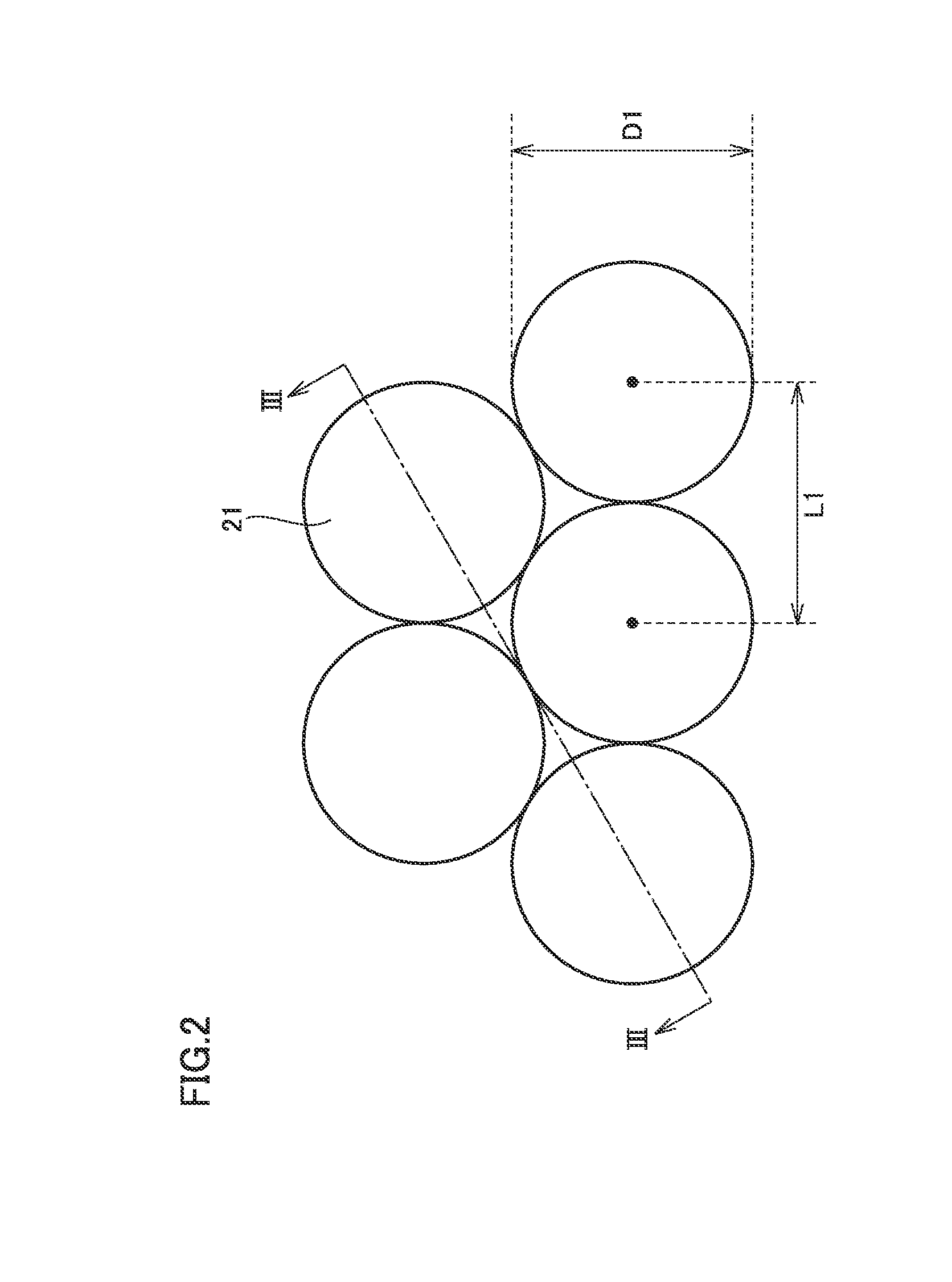
[0099]A semiconductor light emitting element according to a second embodiment of the present invention basically has a structure similar to that of the semiconductor light emitting element shown in FIGS. 1 to 3. However, the semiconductor light emitting element according to the second embodiment of the present invention is different from the semiconductor light emitting element shown in FIGS. 1 to 3, in terms of a configuration of the rear surface of substrate 16. FIG. 6 conceptually shows a planar structure of the rear surface of substrate 16 of the semiconductor light emitting element according to the second embodiment of the present invention. Referring to FIG. 6, in the semiconductor light emitting element according to the second embodiment of the present invention, the rear surface of substrate 16 is used as one example of the light extraction surface, and periodic recessed and projecting structure 21 is formed on the rear surface of substrate 16. A minute recessed and projecti...

example 1

[0143]Based on the structure of the semiconductor light emitting element according to the aforementioned embodiment of the present invention, a semiconductor light emitting element according to Example 1 was fabricated as shown in FIGS. 10 and 11. Specifically, n-type semiconductor layer 15, active layer 13 (light emitting layer) and p-type semiconductor layer 12 were sequentially grown on substrate 16 made of single-crystal AlN by the MOCVD method to form a light emitting element substrate, and positive electrode 11 and negative electrode 14 were arranged at prescribed positions of the light emitting element substrate. An epitaxial layer including the light emitting layer of the semiconductor light emitting element was formed of an AlGaN-based semiconductor similar to that in the aforementioned embodiment, and an emission wavelength of the element was 265 nm.

[0144]An electron beam resist was applied onto a substrate surface (light extraction surface) of the fabricated semiconductor...


PUM


Abstract

The semiconductor light emitting element is a semiconductor light emitting element comprising a semiconductor layer including a light emitting layer, wherein a surface of the semiconductor light emitting element includes a light extraction surface. At least one of the light extraction surface and an interface between two layers having different refractive indexes in the semiconductor light emitting element is provided with a periodic recessed and projecting structure having a period that exceeds 0.5 times as great as a wavelength of light emitted from the light emitting layer, and a minute recessed and projecting structure located on a surface of the periodic recessed and projecting structure and having an average diameter that is not more than 0.5 times as great as the wavelength of the light.

Description

TECHNICAL FIELD[0001]The present invention relates to a semiconductor light emitting element such as a light emitting diode (LED), and particularly to a semiconductor light emitting element improved in light extraction of the light emitted inside the element to the outside, and a method for manufacturing the semiconductor light emitting element.BACKGROUND ART[0002]A semiconductor light emitting element is formed of several layers such as a light emitting layer, an n-type semiconductor layer, a p-type semiconductor layer, an electrode layer, and a supporting substrate. Therefore, the light emitted in the light emitting layer inside the semiconductor element is extracted to the outside after having passed through these several layers. However, when the light passes through a boundary between media having different refractive indexes, i.e., an interface between layers or a surface, a certain rate of reflection occurs inevitably. In addition, when the light passes through or is reflecte...

Claims


Application Information

Patent Timeline
IPC IPC(8): H01L33/58H01L33/32
CPCH01L33/58H01L2933/0058H01L33/32H01L33/22H01L2933/0083H01L33/0062
Inventor INOUE, SHINICHIROTAMARI, NAOKI
Owner STANLEY ELECTRIC CO LTD
Why Eureka
Try Eureka