High-speed interconnects for printed circuit boards

a technology of printed circuit boards and interconnects, which is applied in the direction of high frequency circuit adaptations, circuit masks, and insulating substrate metal adhesion improvement, to achieve the effect of high data transmission rates

Active Publication Date: 2016-06-16
AMPHENOL CORP
View PDF6 Cites 12 Cited by
  • Summary
  • Abstract
  • Description
  • Claims
  • Application Information

AI Technical Summary

Benefits of technology

[0006]The inventors have conceived of new approaches for forming high-speed conductive interconnects on PCBs that can allow higher data transmission rates through a PCB than would be supported on a PCB having a same dielectric layer structure and made by convent

Problems solved by technology

Because attenuation and speed of propagation of a signal along a trace depends on characteristics of the material surrounding that trace, m

Method used


Image

  • High-speed interconnects for printed circuit boards
  • High-speed interconnects for printed circuit boards
  • High-speed interconnects for printed circuit boards

Examples


Embodiment Construction

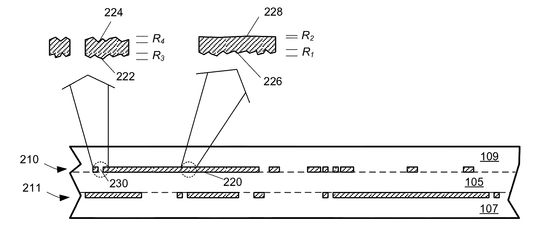
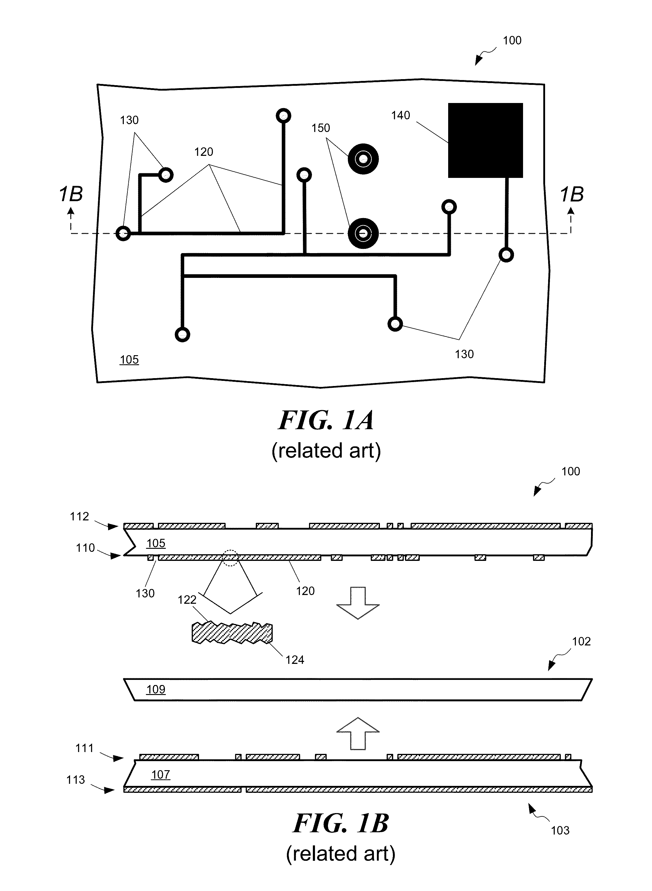
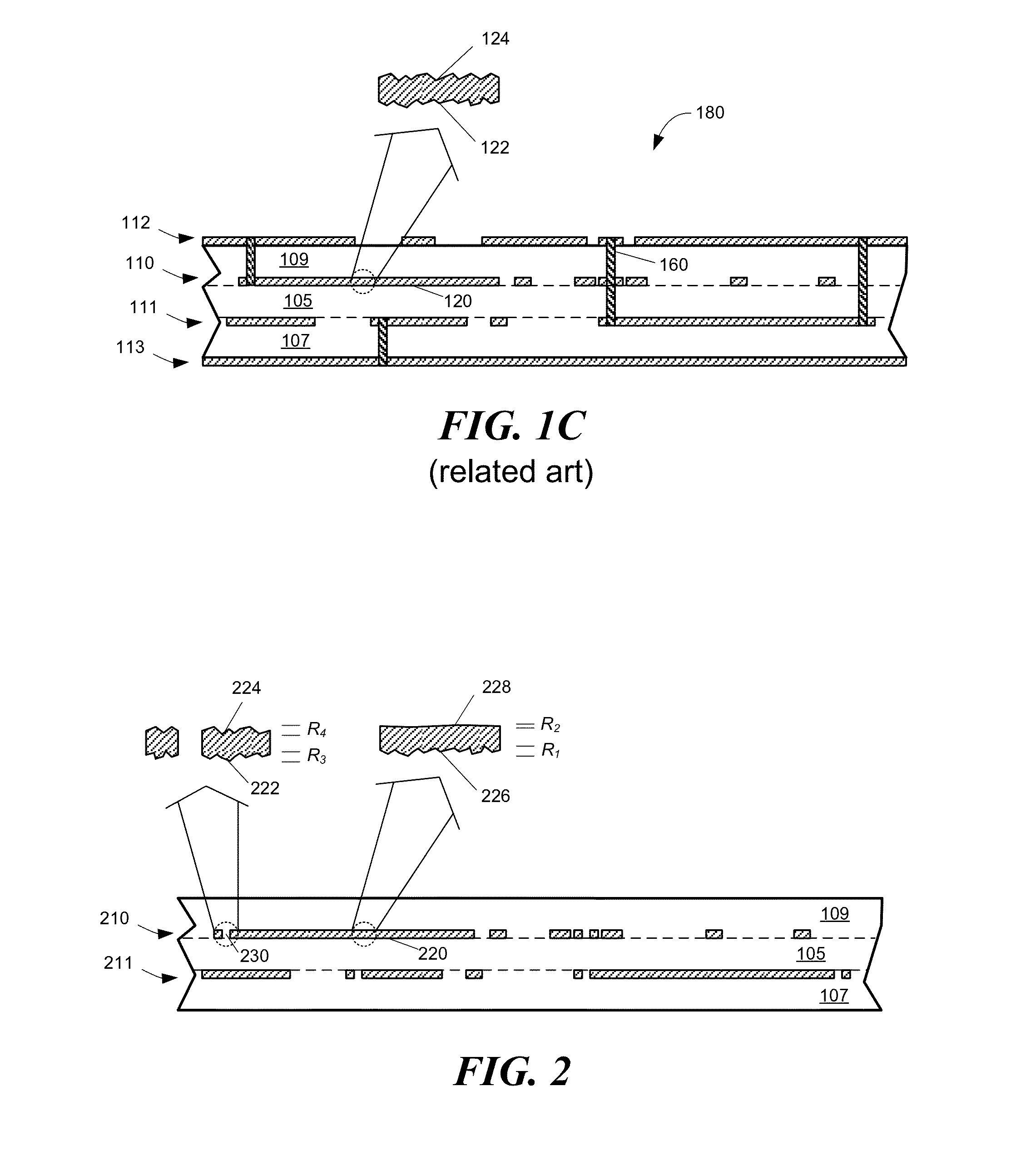
[0031]Recognizing a need for printed circuit boards that can support high-speed data rates, the inventors have conceived of high-speed conductive interconnects and methods for forming the interconnects on PCBs. The inventors recognized that some conductive films and films that have been subjected to conventional surface treatments to improve bonding of the conductive films have appreciable surface roughness that conventionally extends across all patterned interconnects and other features on a PCB. The inventors postulated that this roughness, at high data rates, can contribute undesirable scattering losses, and impede signal transmission. Accordingly, the inventors have developed processes to form high-speed PCB interconnects that have smooth surface regions on at least portions of the interconnects (such as circuit traces or ground planes adjacent traces), for improved signal transmission, and bonding-treated regions at pads and / or other features that improve adhesion to an insulat...


PUM

PropertyMeasurementUnit
Lengthaaaaaaaaaa
Fractionaaaaaaaaaa
Fractionaaaaaaaaaa

Abstract

High-speed interconnects for printed circuit boards and methods for forming the high-speed interconnects are described. A high-speed interconnect may comprise a region of a conductive film having a reduced surface roughness and one or more regions that have been treated for improved bonding with an adjacent insulating layer. Regions of reduced roughness may be used to carry high data rate signals within PCBs. Regions treated for bonding may include a roughened surface, adhesion-promoting chemical treatment, and/or material deposited to improve wettability of the surface and/or adhesion to a cured insulator.

Description

CROSS-REFERENCE TO RELATED APPLICATIONS[0001]This application claims priority to U.S. provisional application Ser. No. 62 / 092,765, titled “High-Speed Interconnects for Printed Circuit Boards,” filed Dec. 16, 2014, which is hereby incorporated by reference in its entirety.FIELD OF THE INVENTION[0002]The invention relates to forming high-speed interconnects for printed circuit boards. In some embodiments, the interconnects can support data rates greater than 50 Gb / s on PCBs.BACKGROUND[0003]Printed circuit boards (PCBs) are widely used in the electronics industry for the manufacture of electronic assemblies. PCBs may be assembled from stacks of dielectric layers (sometimes called “prepreg” layers prior to assembly) and / or laminates or cores. A laminate or core may include at least one planar electrically insulating layer and conductive foils or films on one or both surfaces of the insulating layer. Some of the conductive films may be patterned, using lithographic techniques, to form co...

Claims


Application Information

Patent Timeline
IPC IPC(8): H05K1/02H05K1/09H05K3/38H05K3/46H05K3/00H05K3/22H05K1/03H05K1/11
CPCH05K1/0237H05K2201/0212H05K1/0366H05K1/0326H05K1/034H05K1/0346H05K1/0373H05K1/09H05K1/111H05K1/115H05K3/4685H05K3/0073H05K3/22H05K3/38H05K3/4632H05K2201/0145H05K2201/015H05K2201/0154H05K2201/0158H05K2201/0209H05K1/0298H05K3/382H05K2203/0307H05K1/0242H05K1/116H05K3/202H05K3/383H05K3/384H05K3/385H05K3/388H05K3/389H05K3/4658H05K2203/1194
Inventor HARKNESS, JR., ARTHUR E.KENNY-MCDERMOTT, EVA M.FARINEAU, PAUL W.LAVALLEE, RAYMOND A.FANCHER, MICHAEL
Owner AMPHENOL CORP
Why Eureka
Try Eureka