Schottky barrier diode and method for manufacturing the same
a technology of schottky barrier and diode, which is applied in the direction of basic electric elements, electrical apparatus, and semiconductor devices, can solve problems such as mpsd, and achieve the effects of improving withstand voltage, reducing p-type region ratio, and low withstand voltag
- Summary
- Abstract
- Description
- Claims
- Application Information
AI Technical Summary
Benefits of technology
Problems solved by technology
Method used
Image
Examples
embodiments
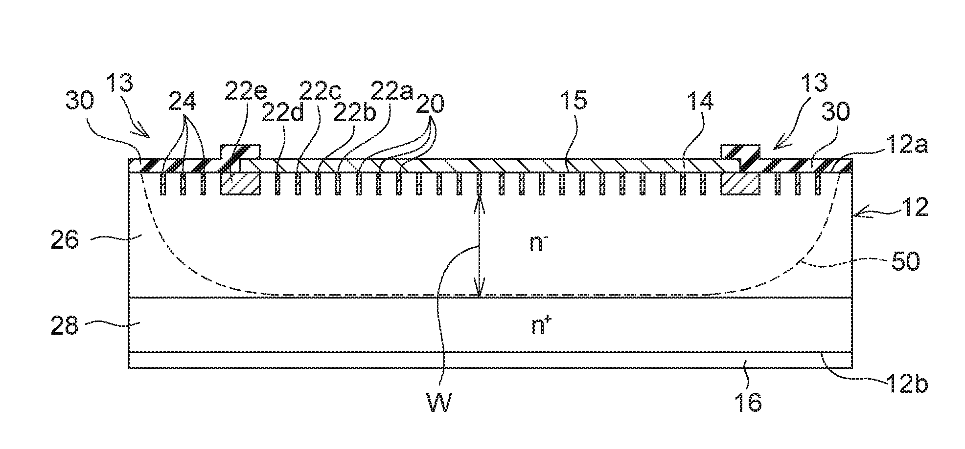
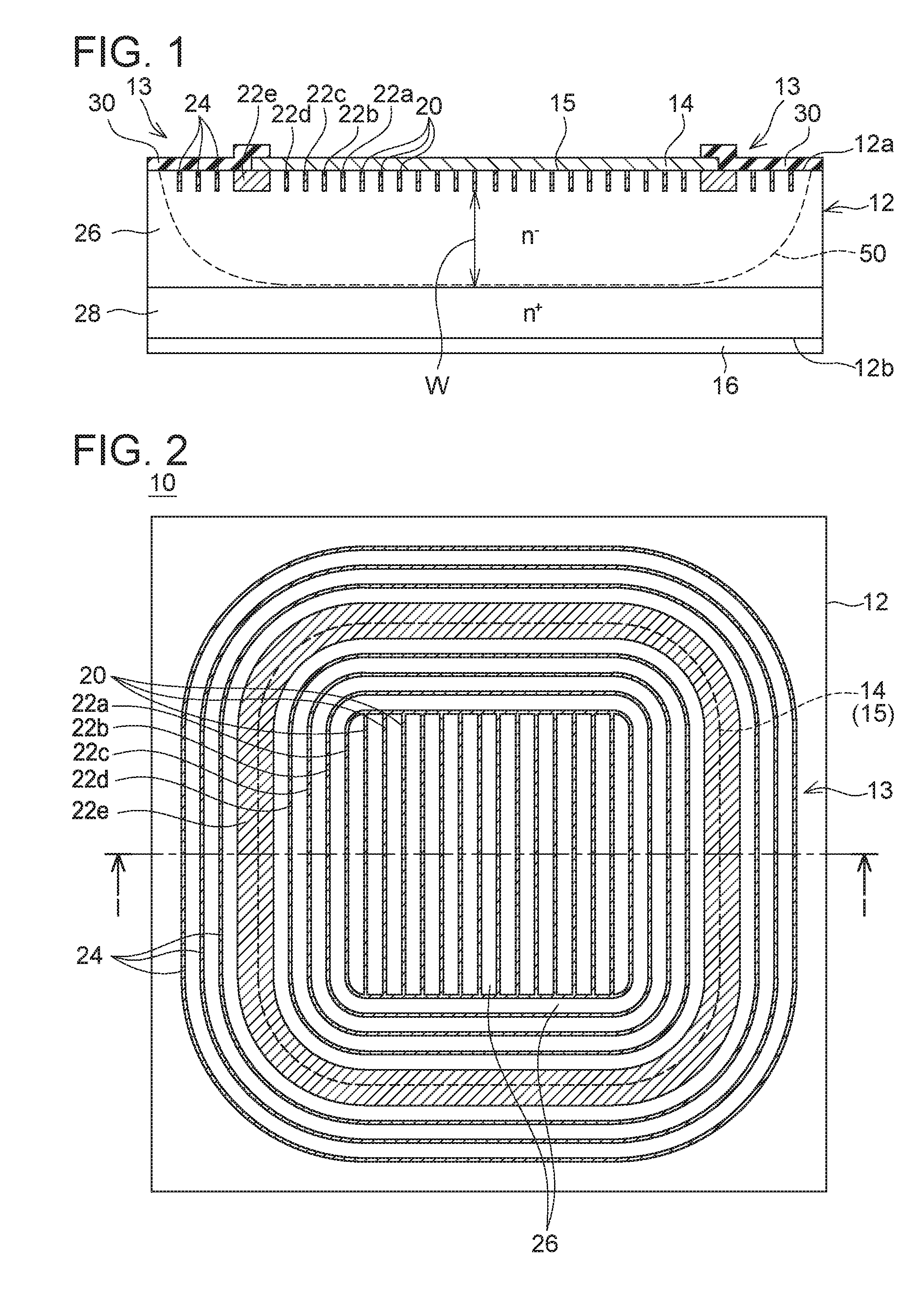
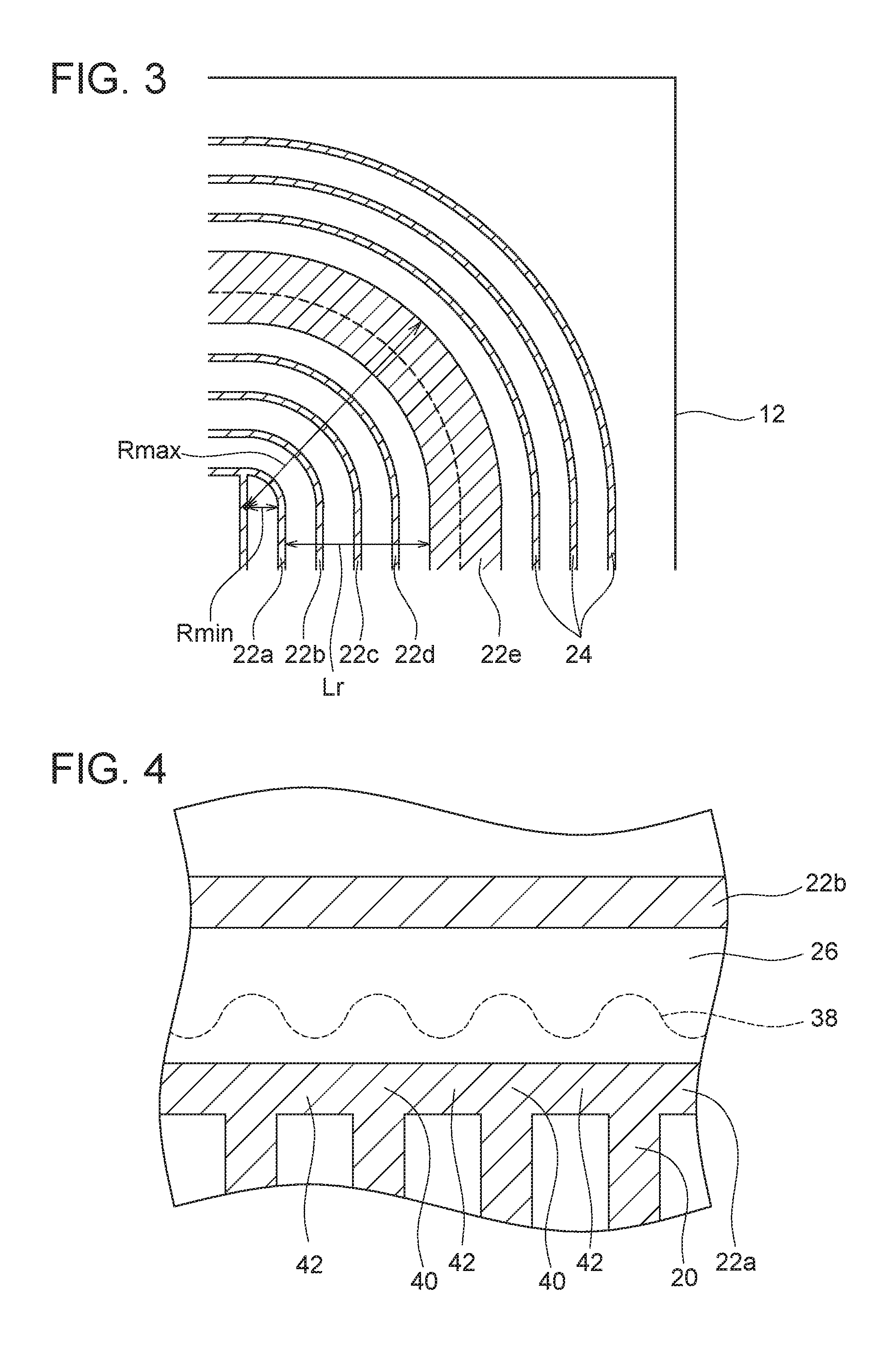
[0016]FIGS. 1 and 2 show an SBD 10 according to an embodiment. The SBD 10 includes a semiconductor substrate 12. In FIG. 2, p-type regions are indicated by diagonal hatching. The semiconductor substrate 12 is made of SiC. The semiconductor substrate 12 has an upper surface 12a on which an anode electrode 14 and an insulating film 30 are provided. A dotted line 14 in FIG. 2 indicates a range in which the anode electrode 14 is provided (i.e. a contact surface 15 where the semiconductor substrate 12 and the anode electrode 14 are in contact with each other). The anode electrode 14 is provided in a central part of the upper surface 12a of the semiconductor substrate 12. A region of the upper surface 12a that is not covered with the anode electrode 14 (i.e. a region on an outer side of the dotted line 14; hereinafter referred to as a “peripheral region 13”) is covered with the insulating film 30. The semiconductor substrate 12 has a lower surface 12b on which a cathode electrode 16 is pr...
PUM
 Abstract
Description
Claims
Application Information


