Display device

Active Publication Date: 2016-07-14
AU OPTRONICS CORP
View PDF3 Cites 23 Cited by
  • Summary
  • Abstract
  • Description
  • Claims
  • Application Information

AI Technical Summary

Benefits of technology

[0008]The display device of the present invention includes the semi-transparent pattern disposed on the second substrate and corresponding to the sealant. The semi-transparent pattern may be used for applying a sealant curing process from a side of the second substrate. Therefore, spacing between the peripheral conductive wires in the peripheral region of the first substrate may be reduced to a minimum value according to design rules and manufacturing abilities, and the area of the peripheral region may be reduced substantially for realizing the narrow border or borderless design.

Problems solved by technology

However, the increased area of the peripheral region conflicts with the narrow border or borderless design of the display device.

Method used


Image

  • Display device
  • Display device
  • Display device

Examples


first embodiment

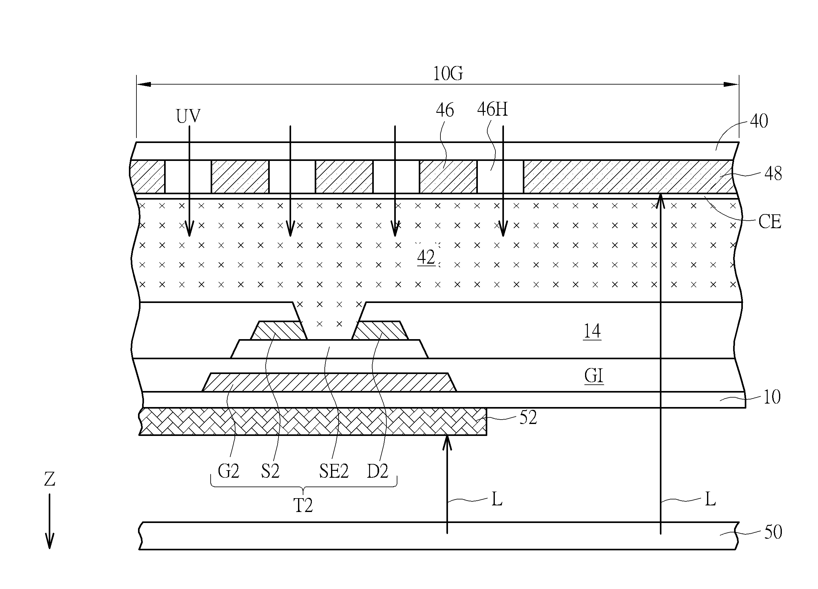
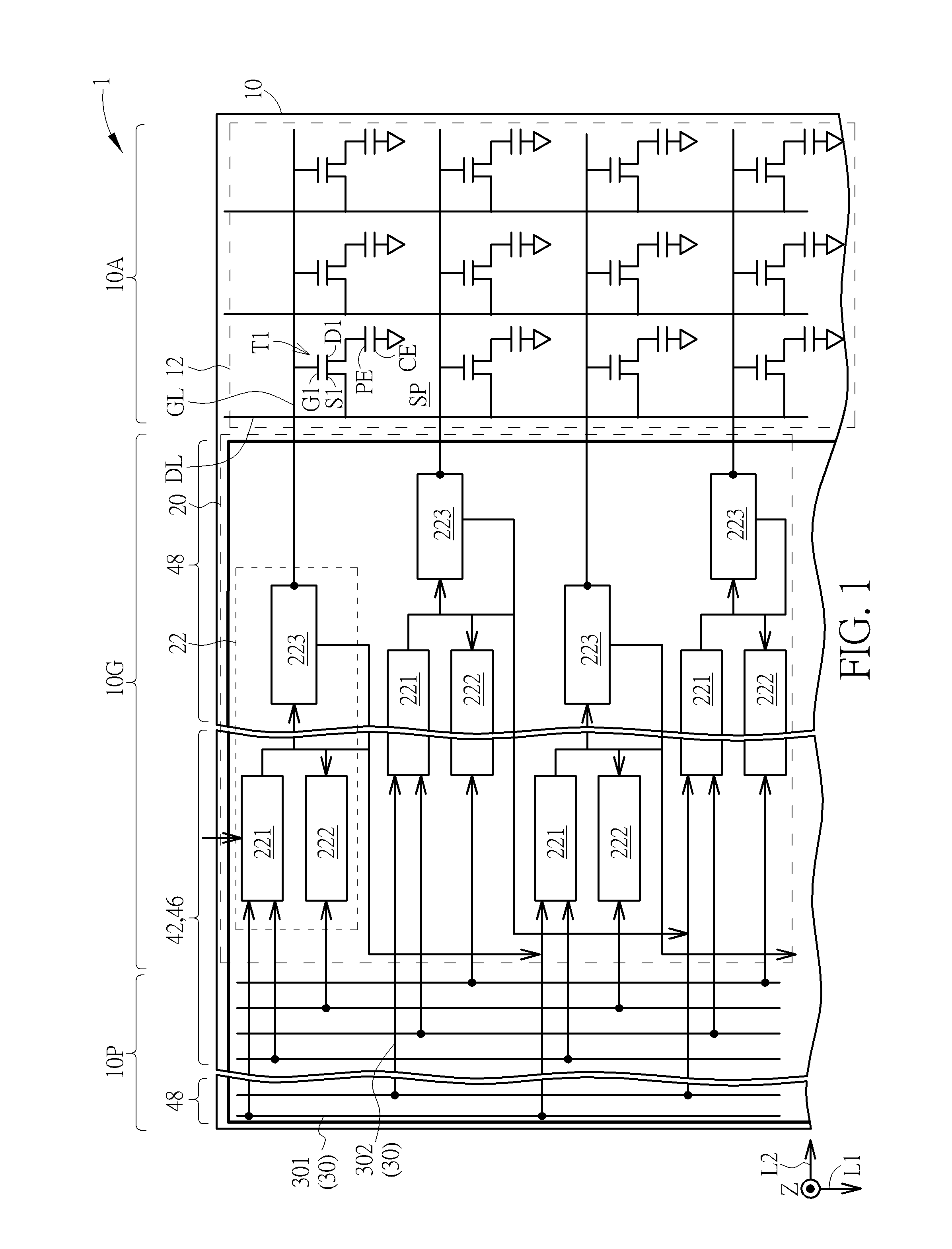
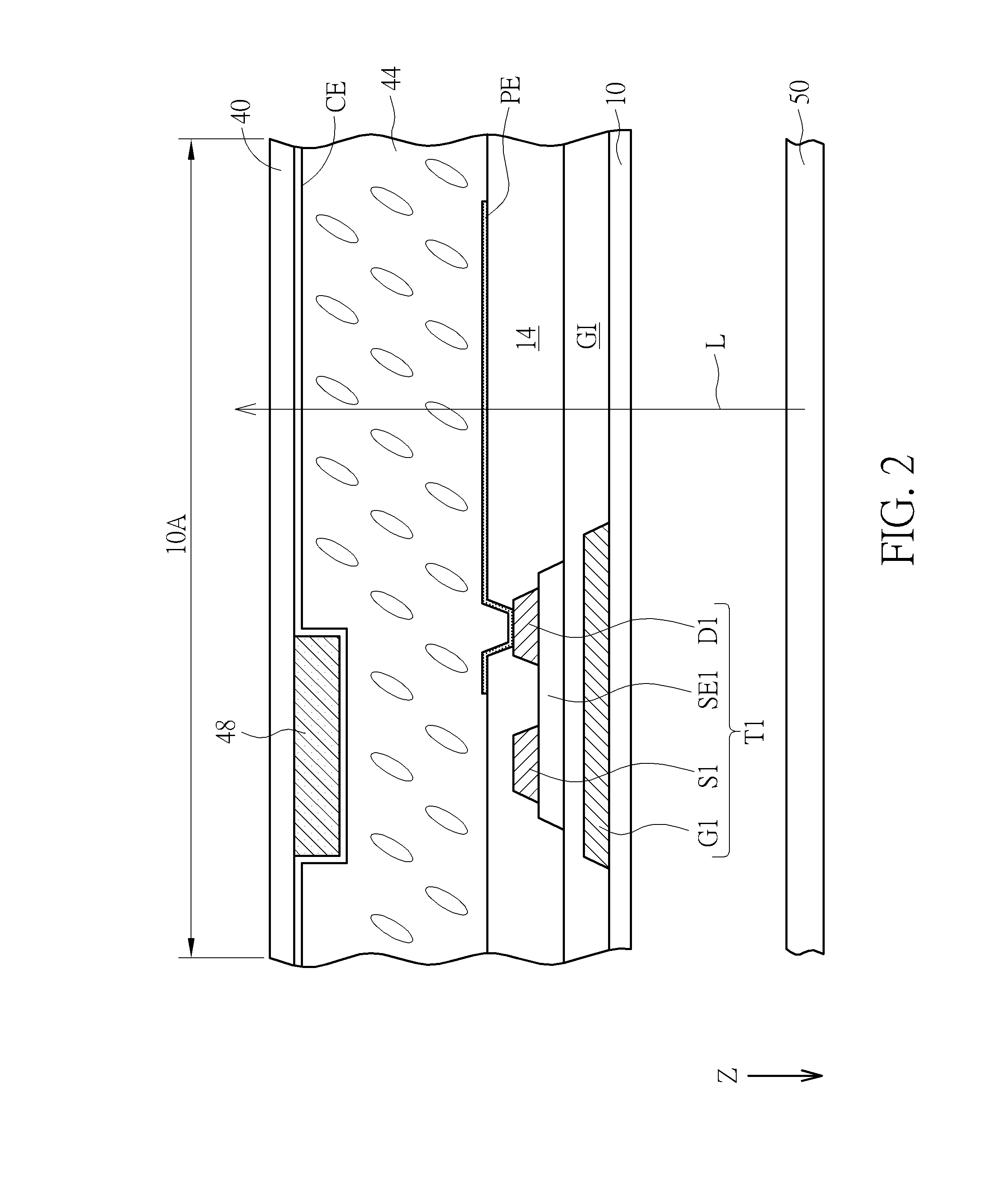
[0021]Please refer to FIGS. 1-5. FIG. 1 is a schematic diagram illustrating a display device according to the present invention. FIG. 2 is a schematic cross-sectional diagram of an active region in the display device of this embodiment. FIG. 3 is a schematic cross-sectional diagram of a gate driver region in the display device of this embodiment.FIG. 4 is a schematic cross-sectional diagram of a peripheral region in the display device of this embodiment. FIG. 5 is a schematic equivalent circuit diagram of a shift register in a gate driver on array circuit of this embodiment. A liquid crystal display device is used as an example of the display device in this embodiment. The liquid crystal display device may include a horizontal electric field liquid crystal display device, a vertical electric field liquid crystal display device, an optically compensated bend (OCB) liquid crystal display device, a cholesteric liquid crystal display device, a blue phase liquid crystal display device or...

second embodiment

[0030]Please refer to FIG. 7. FIG. 7 is a schematic diagram illustrating a display device according to the present invention. As shown in FIG. 7, in a display device 2 of this embodiment, the sealant 42 overlaps a portion of the peripheral conductive wires 30 and the thin film transistor devices T2 in the input units 221 and the pull-down units 222 of all of the shift registers 22 in the vertical direction Z. Additionally, the shape of the semi-transparent pattern 46 substantially overlaps the shape of the sealant 42 in the vertical direction Z. In an exemplary embodiment, the sealant 42 may overlap all of the peripheral conductive wires 30 and the thin film transistor devices T2 in the input units 221 and the pull-down units 222 of all of the shift registers 22, and the sealant 42 does not overlap the pull-up output units 223 of all of the shift registers 22.

third embodiment

[0031]Please refer to FIG. 8. FIG. 8 is a schematic diagram illustrating a display device according to the present invention. As shown in FIG. 8, in a display device 3 of this embodiment, the sealant 42 overlaps a portion of the peripheral conductive wires 30 and all of the shift registers 22 in the vertical direction Z. For example, the sealant 42 overlaps a portion of the peripheral conductive wires 30 and the thin film transistor devices T2 in the input units 221, the pull-down units 222, and the pull-up output units 223 of each of the shift registers 22 in the vertical direction Z. Additionally, the shape of the semi-transparent pattern 46 substantially overlaps the shape of the sealant 42 in the vertical direction Z. In an exemplary embodiment, the sealant 42 may overlap all of the peripheral conductive wires 30 and the thin film transistor devices T2 in the input units 221, the pull-down units 222, and the pull-up output units 223 of all of the shift registers 22.

[0032]Please ...


PUM

PropertyMeasurementUnit
semi-transparentaaaaaaaaaa
transmittanceaaaaaaaaaa

Abstract

A display device includes a first substrate, a gate driver on array (GOA) circuit, a plurality of peripheral conductive wires, a second substrate, a sealant and a semi-transparent pattern. The GOA circuit is disposed in a gate driver region, and includes a plurality of thin film transistor devices. The peripheral conductive wires are disposed in a peripheral region of the first substrate, and the peripheral conductive wires are electrically connected to the GOA circuit. The sealant is disposed in at least a portion of the peripheral region and a portion of the gate driver region, and the sealant overlaps at least a portion of the peripheral conductive wires and a portion of the thin film transistor devices of the GOA circuit in a vertical direction. The semi-transparent pattern is disposed on the second substrate, and a transmittance of the semi-transparent pattern is between 10% and 80%.

Description

BACKGROUND OF THE INVENTION[0001]1. Field of the Invention[0002]The present invention relates to a display device, and more particularly to a display device for realizing narrow border or borderless design.[0003]2. Description of the Prior Art[0004]A conventional display device such as a liquid crystal display device mainly includes an array substrate, a counter substrate, and a liquid crystal layer disposed between these two substrates. The array substrate and the counter substrate are combined by a sealant, and the sealant is used to seal the liquid crystal layer between these two substrates. The array substrate has a display region and a peripheral region disposed outside the display region. A pixel array is disposed in the display region for providing display images, peripheral conductive wires such as gate lines or data lines are disposed in the peripheral region, and driver chips such as gate driver chips or data driver chips are disposed in the peripheral region. Light-shield...

Claims


Application Information

Patent Timeline
Patent Type & Authority Applications(United States)
IPC IPC(8): G02F1/1345G02F1/1339G02F1/1335G02F1/1368
CPCG02F1/13454G02F1/133512G02F1/1339G02F1/1368
Inventor CHEN, CHIA-FANGCHEN, YU-HAOSHEN, PO-YUAN
Owner AU OPTRONICS CORP
Why Eureka
Try Eureka