Adaptive analog-to-digital conversion based on signal prediction

a technology of analog-to-digital conversion and signal prediction, applied in the field of electronic circuits, can solve problems such as noise enhancement, severe impact on the ability to recover a receiver, and reduce the dynamic rang

Active Publication Date: 2016-07-28
RAMBUS INC
View PDF0 Cites 14 Cited by
  • Summary
  • Abstract
  • Description
  • Claims
  • Application Information

AI Technical Summary

Benefits of technology

[0010]Some embodiments described herein feature systems and techniques for adjusting reference voltages of adjustable comparators based on signal prediction. Specifically, some embodiments feature an integrated circuit that comprises (1) sample-and-hold circuitry to sample an input signal based on a clock signal, and to output a sampled voltage for at least a holding period, (2) a plurality of adjustable comparators, wherein each adjustable comparator has a respective reference voltage that is adjustable, and wherein each adjustable comparator outputs a result signal based on comparing the sampled voltage with the adjustable comparator's reference voltage, and (3) control-logic circuitry to predict a voltage range of a future sample of the input signal, and to set reference voltages of the plurality of adjustable comparators based on the predicted voltage range of the future sample of the input signal.

Problems solved by technology

High-speed communication systems often have to combat inter-symbol-interference (ISI) that can severely impact a receiver's capability to recover the transmitted sequence.
Most of these techniques suffer from noise enhancement, error propagation or reduced dynamic range, and generally are not power and space efficient.
Moreover, their performance also degrades considerably in high-speed channels, which can incur losses in excess of 25 dB.
However, the ENOB or the signal to noise ratio of the ADC may degrade if the sampling clock has timing variations.
Digital realization of the equalizer provides better performance compared to its analog counterpart mostly due to better tunability and implementation issues.
The power and size of an ADC increases exponentially with the number of bits, making the implementation of high-speed ADC with a higher number of bits prohibitive.
While the former uses a bank of comparators that grows exponentially with the desired number of bits, the latter requires complicated logics for time interleaving.
Both of these options suffer from power / size inefficiency and may not be suitable for low-power, high-speed applications that require a higher number of bits. FIGS. 1A-1B relate to a conventional flash ADC.
These ADCs consume a lot of power and use up a large amount of chip area because they require O(2N) comparators.
This makes SAR ADC unsuitable for high-speed applications where N additional clock cycles are needed for N bit resolution.

Method used


Image

  • Adaptive analog-to-digital conversion based on signal prediction
  • Adaptive analog-to-digital conversion based on signal prediction
  • Adaptive analog-to-digital conversion based on signal prediction

Examples


Embodiment Construction

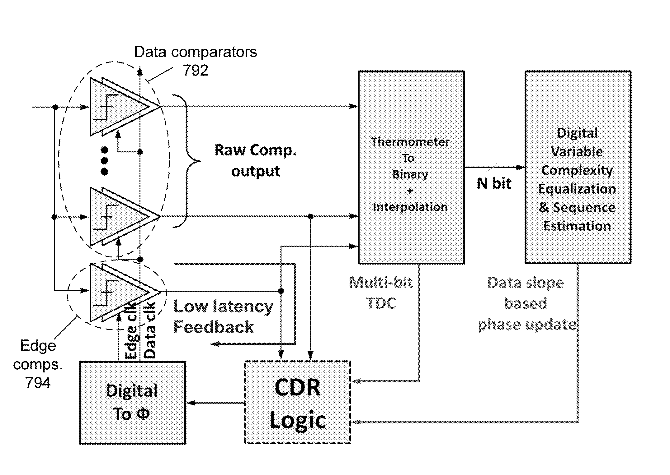
[0028]Some embodiments described herein feature a unified approach to designing and optimizing the ADC, CDR and equalizer by exchanging information among them. The complementary nature of the design offers a wide variety of power / complexity / size trade-offs that can support a broad range of channels in a single receiver realization.

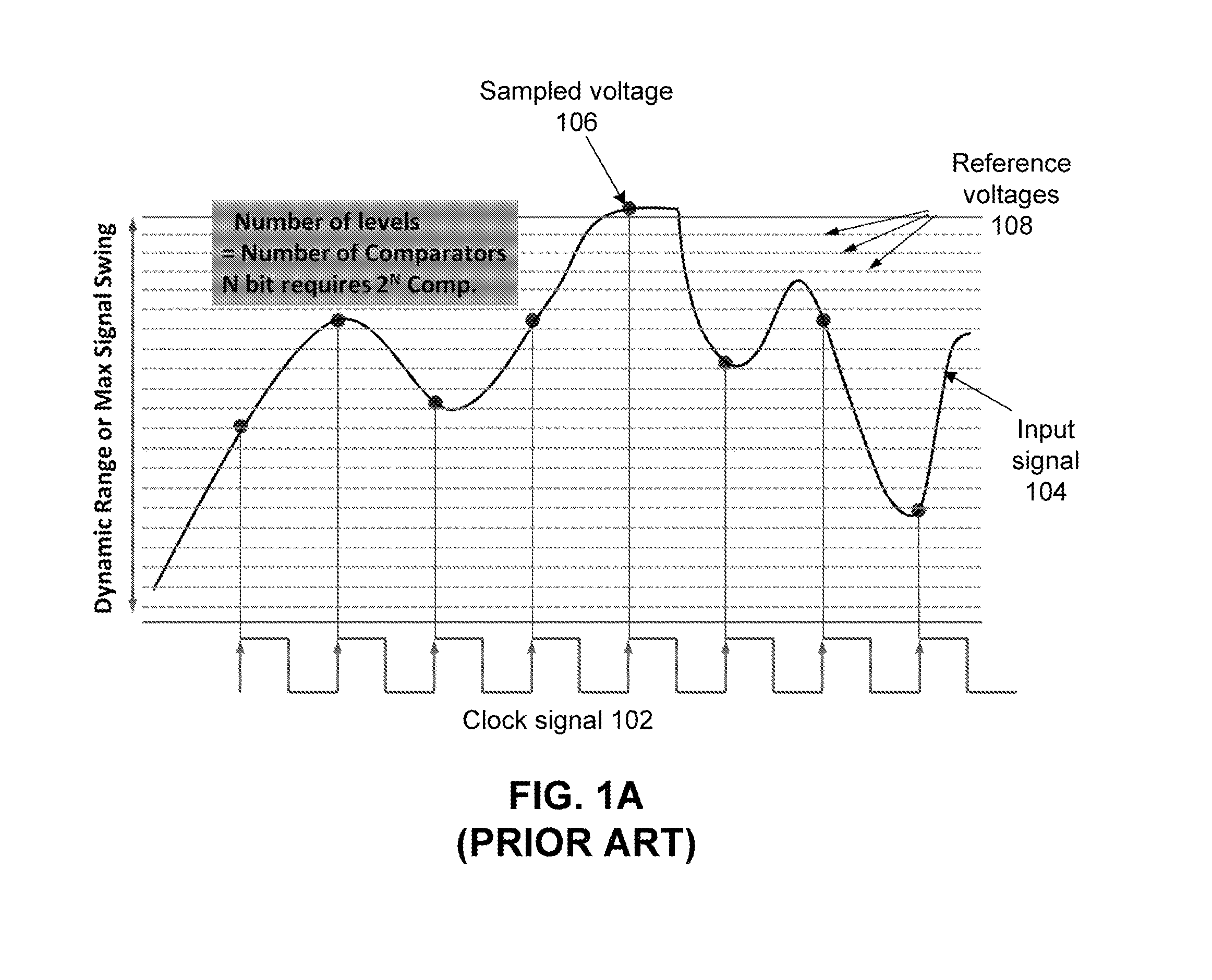
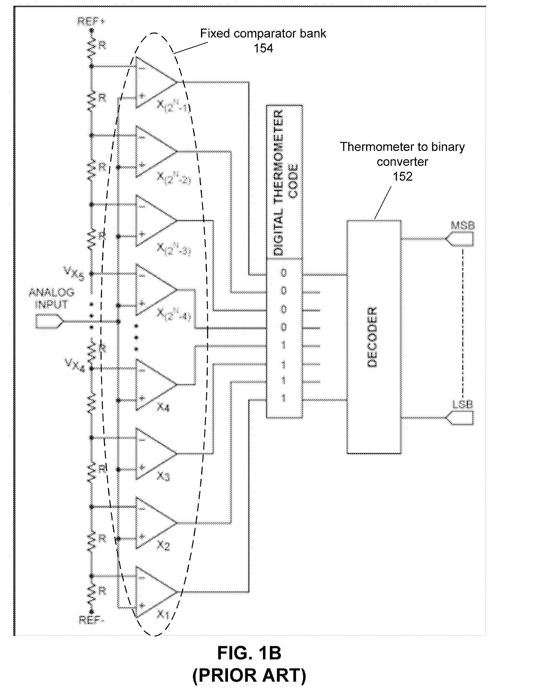
[0029]Frequency dependent loss of the channel causes distortion known as ISI. This can be captured in a single bit response (SBR). FIG. 2A illustrates an SBR in accordance with some embodiments described herein. In FIG. 2A, a lone ‘1’ is sent from the transmitter side and signal 202 is received at the receiver. Note that the perfect UI wide pulse is spread out at the receiver end and corrupts the symbols before and after the ‘1’. In particular, residual voltages on ‘0’ locations prior to the main cursor are known as pre-cursor ISI and residual voltages on ‘0’ locations after the main cursor are known as post-cursor ISI. In simple words, the ISI is the resi...


PUM


Abstract

Methods and apparatuses are described for performing adaptive analog-to-digital conversion and time-to-delay conversion by using signal prediction to adjust reference voltages of adjustable comparators.

Description

BACKGROUND[0001]1. Technical Field[0002]This disclosure relates to electronic circuits. Specifically, this disclosure relates to electronic circuits for analog-to-digital conversion (ADC) and time-to-delay conversion (TDC).[0003]2. Related Art[0004]High-speed communication systems often have to combat inter-symbol-interference (ISI) that can severely impact a receiver's capability to recover the transmitted sequence. Usually an equalization technique is employed at the receiver to correct the channel induced interference. The ISI is generally data dependent and can include signal components with contributions based on prior (pre-cursor) and post (post-cursor) received signals. Various techniques exist, both in the literature and practice, to address pre-cursor and post-cursor ISI. Usually performed at the receiver, existing equalization techniques include attempts to undo the channel introduced interference as well as reconstruction of the ISI through detected signals. With the know...

Claims


Application Information

Patent Timeline
Patent Type & Authority Applications(United States)
IPC IPC(8): G11C27/02G05F1/10H04L25/03H03M1/12H04L7/033H03L5/00H03M1/38
CPCG11C27/02H03L5/00G05F1/10H04L25/03006H03M1/124H04L7/0332H03M1/38H03M1/1245H03M1/1255H03M1/361H04L7/0087H04L7/033H04L7/0334H04L25/069H03M1/002H03L7/0807
Inventor HOSSAIN, MASUMMOHAMMAD, MARUF H.
Owner RAMBUS INC
Why Eureka
Try Eureka