Piezoelectric element and method for manufacturing piezoelectric element

a piezoelectric element and piezoelectric technology, applied in piezoelectric/electrostrictive/magnetostrictive devices, mechanical vibration separation, electrical apparatus, etc., can solve the problems of high manufacturing cost, complicated manufacturing process, and high cost of soi substrate, and achieve high efficiency and high stability. , the effect of simple process

Inactive Publication Date: 2016-08-18
FUJIFILM CORP
View PDF4 Cites 63 Cited by
  • Summary
  • Abstract
  • Description
  • Claims
  • Application Information

AI Technical Summary

Benefits of technology

[0053]According to the fifteenth aspect, a piezoelectric element which operates with high efficiency can be manufactured through a simple process. In the method for manufacturing a piezoelectric element according to the fifteenth aspect, features specified in the second to fourteenth aspects can be appropriately combined with each other.
[0054]According...

Problems solved by technology

Therefore, the manufacturing process is complicated, and the manufacturing costs are high.
In addition, in the configuration disclosed in JP2013-80886A using the SOI substrate, the SOI substrate is expensive.
Therefore, warping is likely to occur due to a temperature variation, and drive characteristics or a sensor output is likely to vary.
Therefore, the actuator cannot be used as a driving source of a device having a high resonance frequency.
In addition, in the configuration in which the laminated piezoelectric body which d...

Method used


Image

  • Piezoelectric element and method for manufacturing piezoelectric element
  • Piezoelectric element and method for manufacturing piezoelectric element
  • Piezoelectric element and method for manufacturing piezoelectric element

Examples


modification example 1

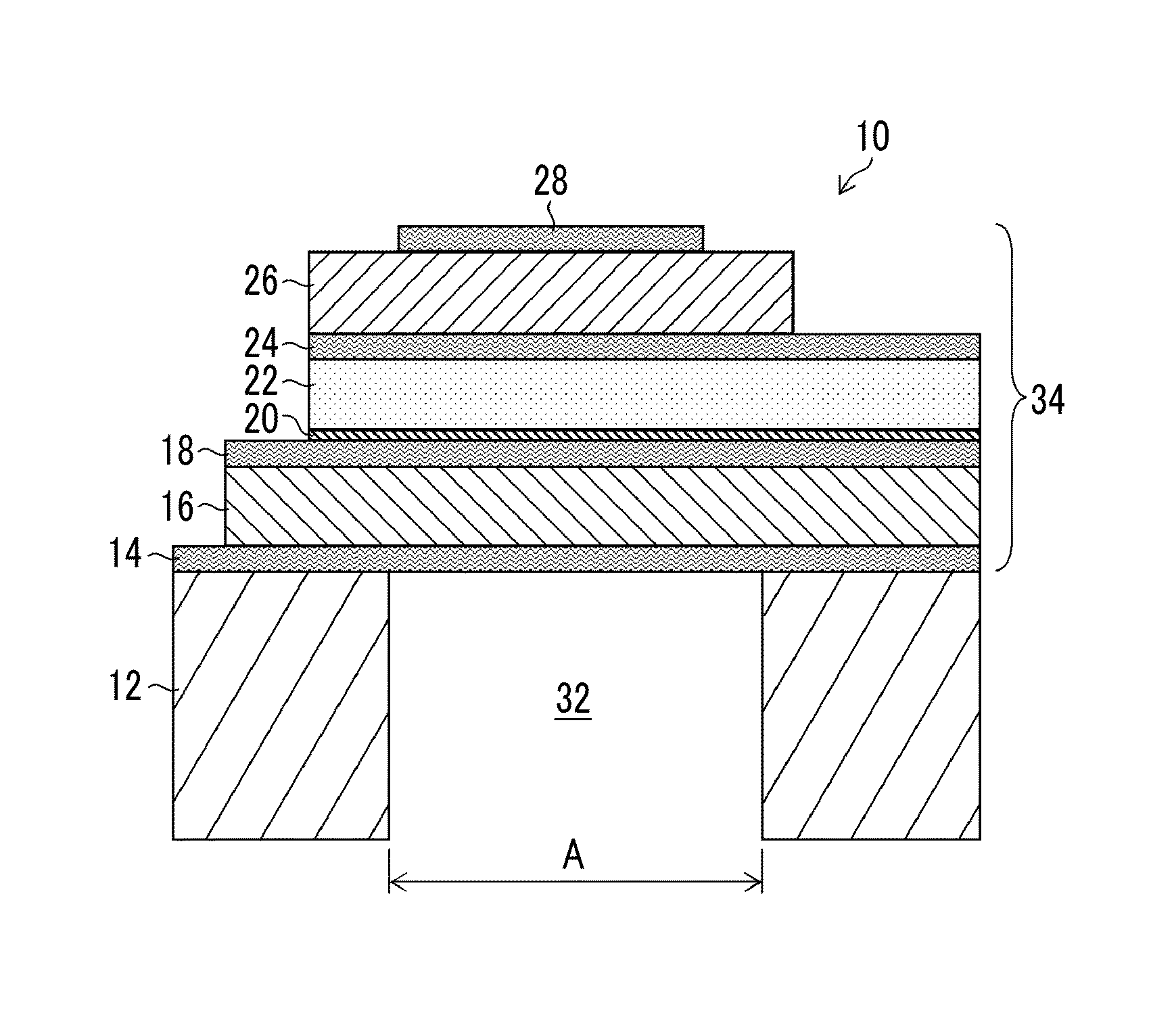
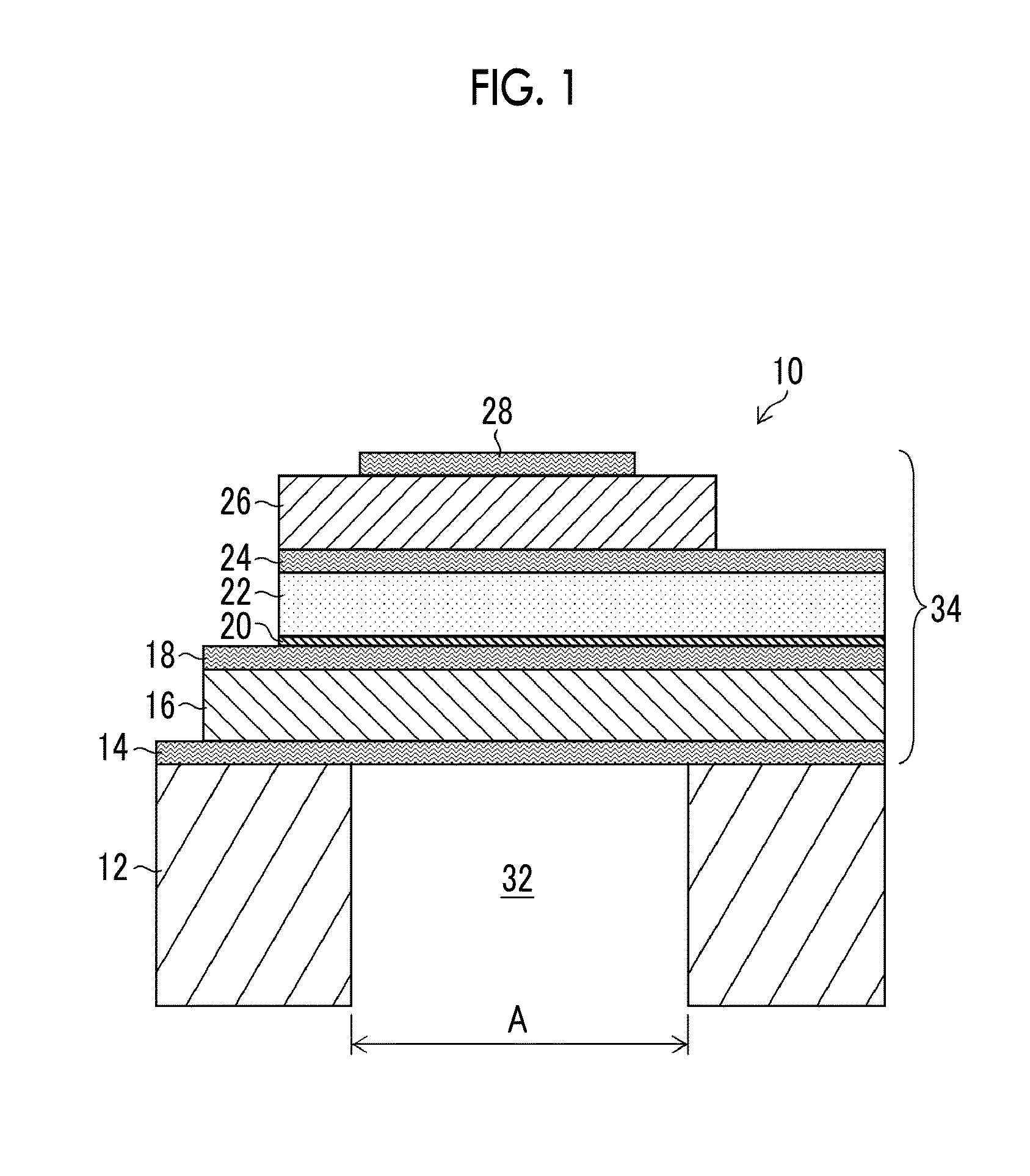
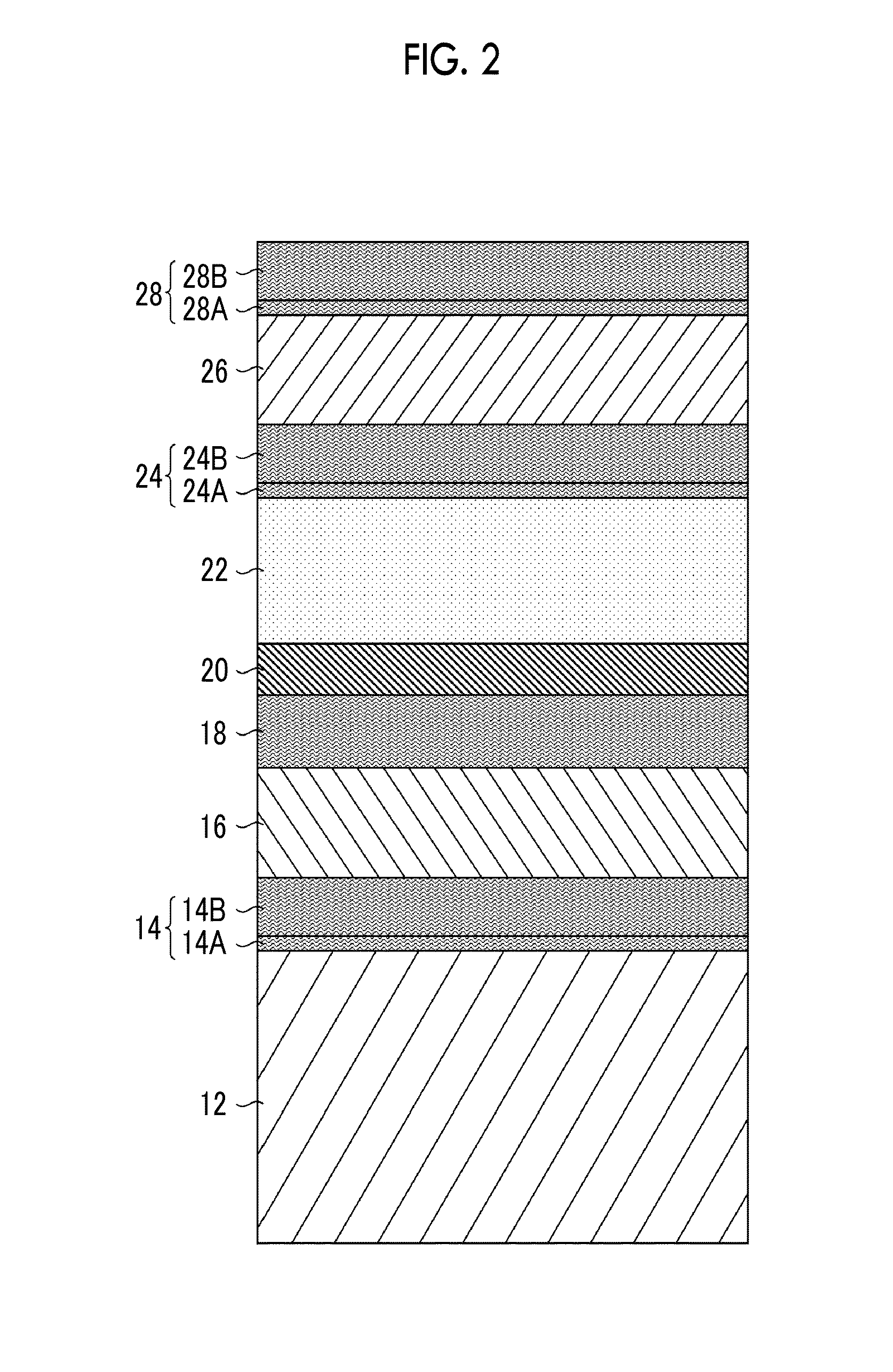
[0184]In the above-described description, Si is used as the material of the interlayer 22. However, in another example, a material obtained by adding Ni to Si was used to form the interlayer 22 having the same structure as shown in FIG. 1 using a sputtering method. However, the addition amount of Ni is lower than 50% by mass. Depending on the composition ratio of Si and Ni, the thermal expansion coefficient of the Si—Ni material ranges between the thermal expansion coefficient of Si (2.4 ppm / ° C.) and the thermal expansion coefficient of Ni (12.8 ppm / ° C.). The interlayer 22 which is formed of the material containing Si as a major component and further containing Ni is conductive and can function as a common electrode for the first piezoelectric film 16 and the second piezoelectric film 26. As long as Si is contained as a major component, a metal element other than Ni may be added or a combination of plural kinds of metal elements may be added to Si.

modification example 2

[0185]FIG. 1 shows the structure in which the two piezoelectric films (16, 26) are laminated with the interlayer 22 interposed therebetween. In the practice of the present invention, a configuration may be adopted in which three or more piezoelectric films are laminated by further laminating a piezoelectric film on the fourth electrode 28.

modification example 3

[0186]In a device, either or both of the first piezoelectric film 16 and the second piezoelectric film can operate using a positive piezoelectric effect. In addition, in a device, either or both of the first piezoelectric film 16 and the second piezoelectric film can operate using an inverse piezoelectric effect. In addition, in the single piezoelectric element 10, a portion using a positive piezoelectric effect and a portion using an inverse piezoelectric effect can be combined with each other.


PUM


Abstract

Provided are a piezoelectric element having high stability, which operates with high efficiency, and a method for manufacturing the piezoelectric element. The piezoelectric element (10) has a laminate structure in which a first electrode (14), a first piezoelectric film (16), a second electrode (18), an adhesion layer (20), an interlayer (22), a third electrode (24), a second piezoelectric film (26), and a fourth electrode (28) are laminated in this order on a silicon substrate (12). The interlayer (22) is formed of a material different from that of the second electrode (18) and has a thickness of 0.4 μm to 10 μm. A device having a diaphragm structure or a cantilever structure is formed by removing a part of the silicon substrate (12). The respective layers (14 to 28) laminated on the silicon substrate (12) can be formed using a thin film formation method represented by a vapor phase epitaxial method.

Description

CROSS-REFERENCE TO RELATED APPLICATIONS[0001]The present application is a Continuation of PCT International Application No. PCT / JP2014 / 077958 filed on Oct. 21, 2014 claiming priority under 35 U.S.C §119(a) to Japanese Patent Application No. 2013-223376 filed on Oct. 28, 2013. Each of the above applications is hereby expressly incorporated by reference, in their entirety, into the present application.BACKGROUND OF THE INVENTION[0002]1. Field of the Invention[0003]The present invention relates to a piezoelectric element and a method for manufacturing a piezoelectric element. In particular, the present invention relates to a piezoelectric element using a piezoelectric thin film material, which is used for various uses such as an actuator, a sensor, or a power generation device, and a method for manufacturing the same.[0004]2. Description of the Related Art[0005]As a piezoelectric actuator of the related art, a unimorph actuator having a structure in which an upper electrode, a piezoele...

Claims


Application Information

Patent Timeline
IPC IPC(8): H01L41/083H01L41/08H01L41/27H01L41/047
CPCH01L41/0471B06B1/0611H01L41/081H01L41/0815H01L41/0831H01L41/094H01L41/0973H01L41/1132H01L41/1136H01L41/1138H01L41/29H01L41/297H01L41/316H01L41/319H01L41/0805H01L41/083H01L41/27B81C1/00158H01L41/0478H10N30/871H10N30/878H10N30/1051H10N30/501H10N30/2042H10N30/2047H10N30/05H10N30/067H10N30/076H10N30/50
Inventor FUJII, TAKAMICHINAONO, TAKAYUKI
Owner FUJIFILM CORP
Why Eureka
Try Eureka