Multiple Integrated Tips Scanning Probe Microscope

a scanning probe and integrated technology, applied in scanning probe microscopy, instruments, measurement devices, etc., can solve the problems of inaccessible fundamental phenomena of thin film materials and devices, inability to characterize the effects of dislocation and grain boundaries of thin films, and limited single-tip spms

Inactive Publication Date: 2016-09-01
XALLENT INC
View PDF17 Cites 8 Cited by
  • Summary
  • Abstract
  • Description
  • Claims
  • Application Information

AI Technical Summary

Benefits of technology

[0007]The present disclosure is directed to a multiple integrated tips (MiT) scanning probe microscope for the characterization of thin films and devices. The MiT scanning probe microscope is a platform that integrates mechanical and electrical functionality in a monolithically-fabricated nano-structure which is tailored and functionalized to the specific investigation. The MiT probe provides two or more monolithically integrated cantilever tips that can be placed within nanometers of each other, with monolithically integrated capacitive actuators, sensors, and transistors to amplify signals. As a result, the MiT SPM is able to perform atomic force microscopy without the need for laser tip alignment. Further, the MiT SPM is capable of nanoprobing surfaces where at least two of the integrated tips are in direct contact or in close proximity with the sample.

Problems solved by technology

However, single-tip SPMs are limited to static measurements such as the local density of states and near-sample surface effects.
As a result, a range of fundamental phenomena that exist in thin film materials and devices are inaccessible.
As just one example, the effects of dislocations and grain boundaries in thin films cannot be characterized, as the ability to perform trans-conductance (conduction between two tips) measurements at the nanoscale is a critical gap.
However, there have been significant challenges to engineering a suitable multiple-tips SPM.
These platforms are complex, difficult to actuate, and have limited scale-down.
They are also prohibitively expensive to manufacture.

Method used


Image

  • Multiple Integrated Tips Scanning Probe Microscope
  • Multiple Integrated Tips Scanning Probe Microscope
  • Multiple Integrated Tips Scanning Probe Microscope

Examples


Embodiment Construction

[0049]The present disclosure describes various embodiments of a multiple integrated tips scanning probe microscope for the characterization of thin films and devices. The MiT-SPM enables nanoscale atomic imaging, as well as electrical probing of trans-conductance, in ambient air without requiring a scanning electron microscope. The device provides for detailed studies of transport mechanisms in thin film materials and devices.

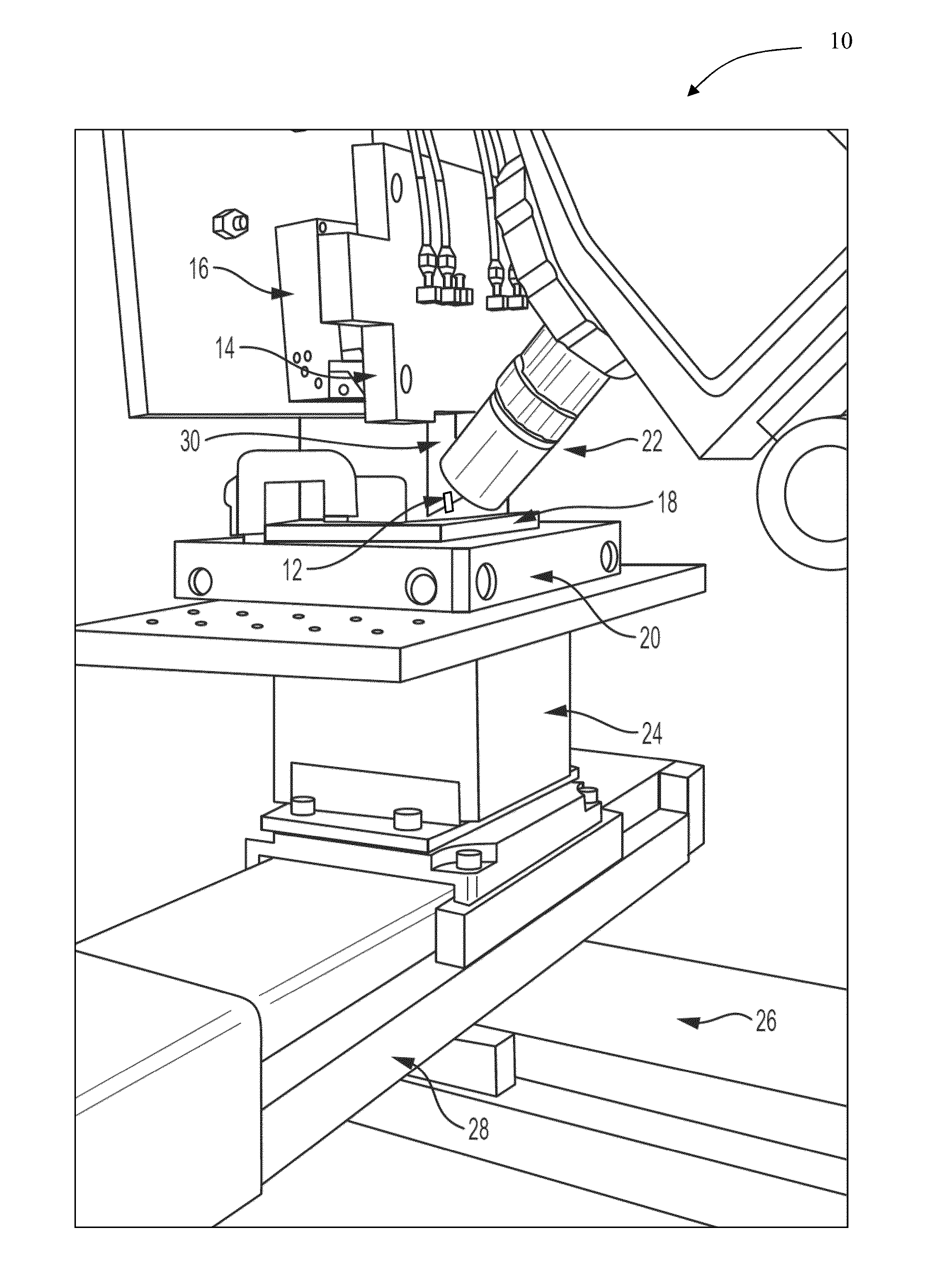
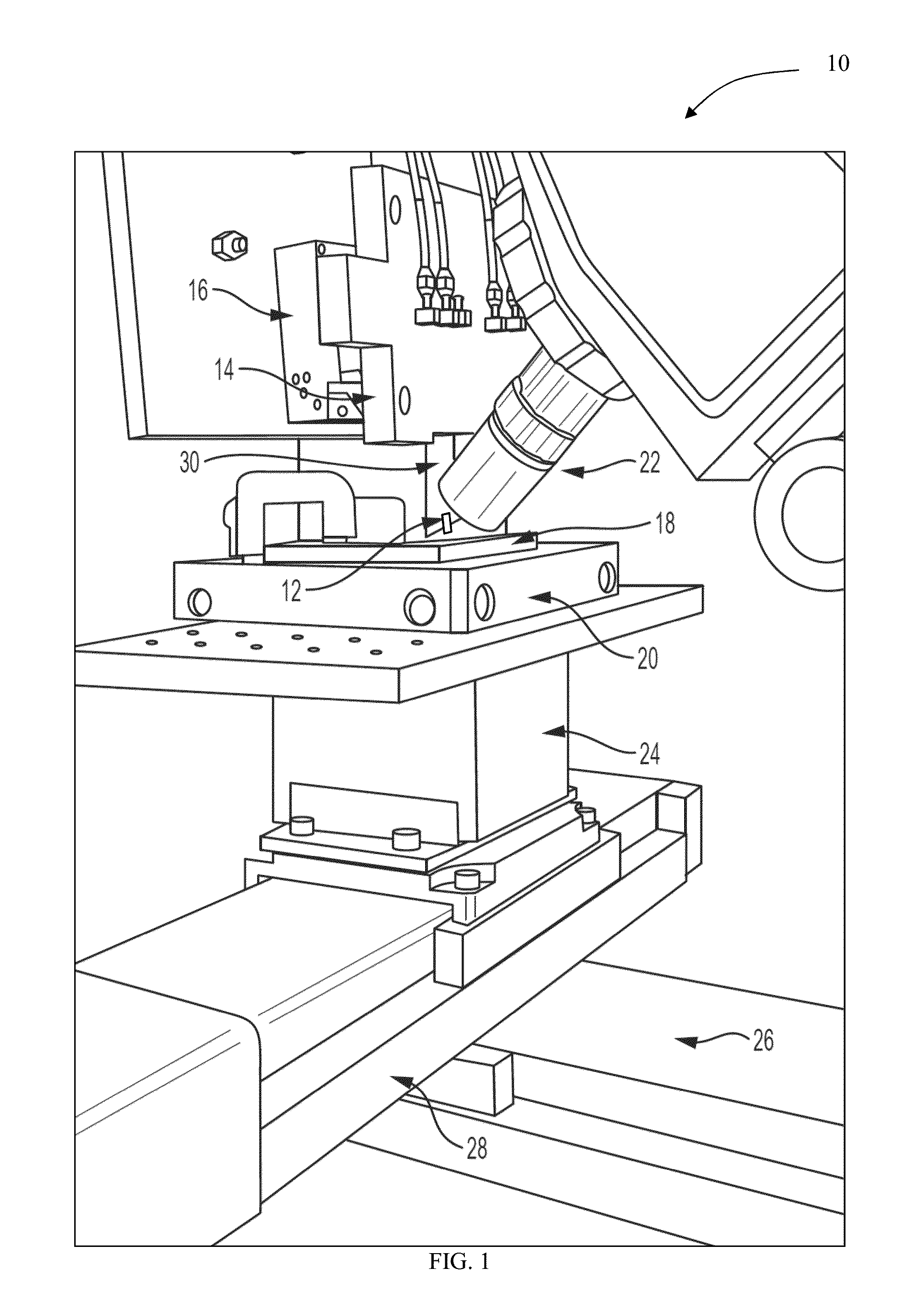
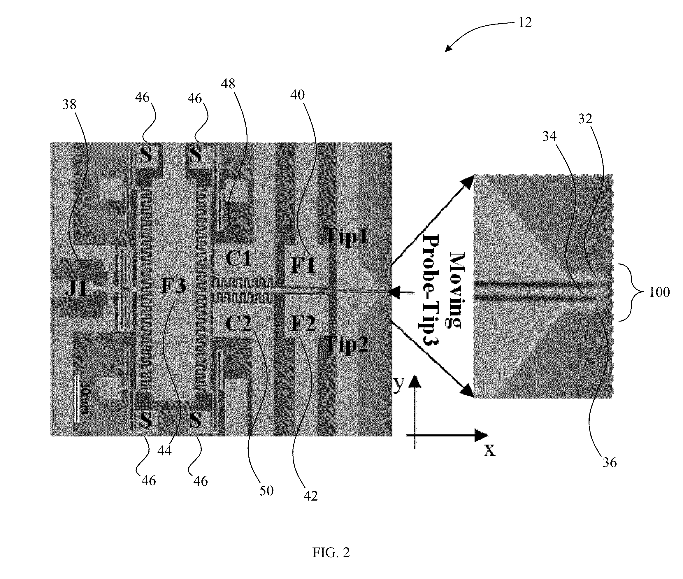
[0050]Referring now to the drawings, wherein like reference numerals refer to like parts throughout, there is seen in FIG. 1, in one embodiment, a multiple integrated tip scanning probe microscope system 10. The MiT-SPM system includes the MiT probe 12, which can be wire-bonded to a printed circuit board (PCB) 30. The MiT-SPM also includes a scanning probe head 14, which houses the transduction electronics including the transimpedance amplifier (TIA) which converts the tunneling current into voltage, as discussed in greater detail below. A rotating stage 16 ali...


PUM


Abstract

Device and system for characterizing samples using multiple integrated tips scanning probe microscopy. Multiple Integrated Tips (MiT) probes are comprised of two or more monolithically integrated and movable AFM tips positioned to within nm of each other, enabling unprecedented micro to nanoscale probing functionality in vacuum or ambient conditions. The tip structure is combined with capacitive comb structures offering laserless high-resolution electric-in electric-out actuation and sensing capability and novel integration with a Junction Field Effect Transistor for signal amplification and low-noise operation. This “platform-on-a-chip” approach is a paradigm shift relative to current technology based on single tips functionalized using stacks of supporting gear: lasers, nano-positioners and electronics.

Description

CROSS-REFERENCE TO RELATED APPLICATIONS[0001]This application claims priority to U.S. Provisional Patent Application Ser. No. 62 / 121,174, filed on Feb. 26, 2015 and entitled “Multiple Integrated Tip Scanning Probe Microscope,” the entire disclosure of which is incorporated herein by reference.FIELD OF THE INVENTION[0002]The present disclosure is directed generally to a multiple integrated tips scanning probe microscope for the characterization of thin films and devices.BACKGROUND[0003]Single-tip Scanning Probe Microscopes (SPM), such as the Scanning Tunneling Microscope (STM) and Atomic Force Microscope (AFM), are critical tools for the investigation of structural and electronic properties of thin film materials and devices. For example, these single-tip SPMs form one or more images of a thin film material or device using a physical probe that scans the target.[0004]However, single-tip SPMs are limited to static measurements such as the local density of states and near-sample surfac...

Claims


Application Information

Patent Timeline
Patent Type & Authority Applications(United States)
IPC IPC(8): G01Q20/02G01Q30/02
CPCG01Q30/025G01Q20/02G01Q10/045G01Q20/04G01Q60/04G01Q60/30G01Q70/06
Inventor AMPONSAH, KWAME
Owner XALLENT INC
Why Eureka
Try Eureka