Semiconductor device and method for manufacturing the same

a semiconductor and semiconductor technology, applied in semiconductor devices, diodes, electrical devices, etc., to achieve the effect of reducing crystal defect density, and suppressing on-state voltage variations

Inactive Publication Date: 2016-09-01
TOYOTA JIDOSHA KK
View PDF1 Cites 10 Cited by
  • Summary
  • Abstract
  • Description
  • Claims
  • Application Information

AI Technical Summary

Benefits of technology

[0011]This manufacturing method includes implanting charged particles into the semiconductor substrate from the front surface side. Such implantation of charged particles causes crystal defects to be formed at a highest density at a position where the charged particles stop, thus causing the first lifetime control layer to be formed. After completion of the semiconductor device, the first lifetime control layer is positioned in the range closer to the rear surface than the intermediate portion of the semiconductor substrate in the thickness direction. Further, crystal defects are also formed in a region between the first lifetime control layer and the front surface of the semiconductor substrate (i.e., a region through which the charged particles pass), albeit at a lower density than in the first lifetime control layer. For this reason, a crystal defect density is higher in the region closer to the front surface than the first lifetime control layer than in the region closer to the rear surface. This manufacturing method includes forming the emitter region, the body region, and the gate electrode in the region closer to the front surface of the semiconductor substrate and forming the collector region in the region closer to the rear surface. That is, the collector region is formed in a region in which a crystal defect density is low. For this reason, this manufacturing method makes it possible to suppress variations in the on-state voltages of the IGBTs among semiconductor devices that are manufactured. In this way, in this manufacturing method, charged particles are implanted into the semiconductor substrate from the front surface side so as to form the first lifetime control layer. That is, this manufacturing method does not include a step of implanting charged particles (i.e., charged particles for forming crystal defects) from the rear surface side into a range in the semiconductor substrate in which the collector region is formed. This makes it possible to lower the crystal defect density in the collector region, thus making it possible to suppress variations in the on-state voltages of the IGBTs.

Problems solved by technology

Such implantation of charged particles causes crystal defects to be formed at a highest density at a position where the charged particles stop, thus causing the first lifetime control layer to be formed.

Method used


Image

  • Semiconductor device and method for manufacturing the same
  • Semiconductor device and method for manufacturing the same
  • Semiconductor device and method for manufacturing the same

Examples


Embodiment Construction

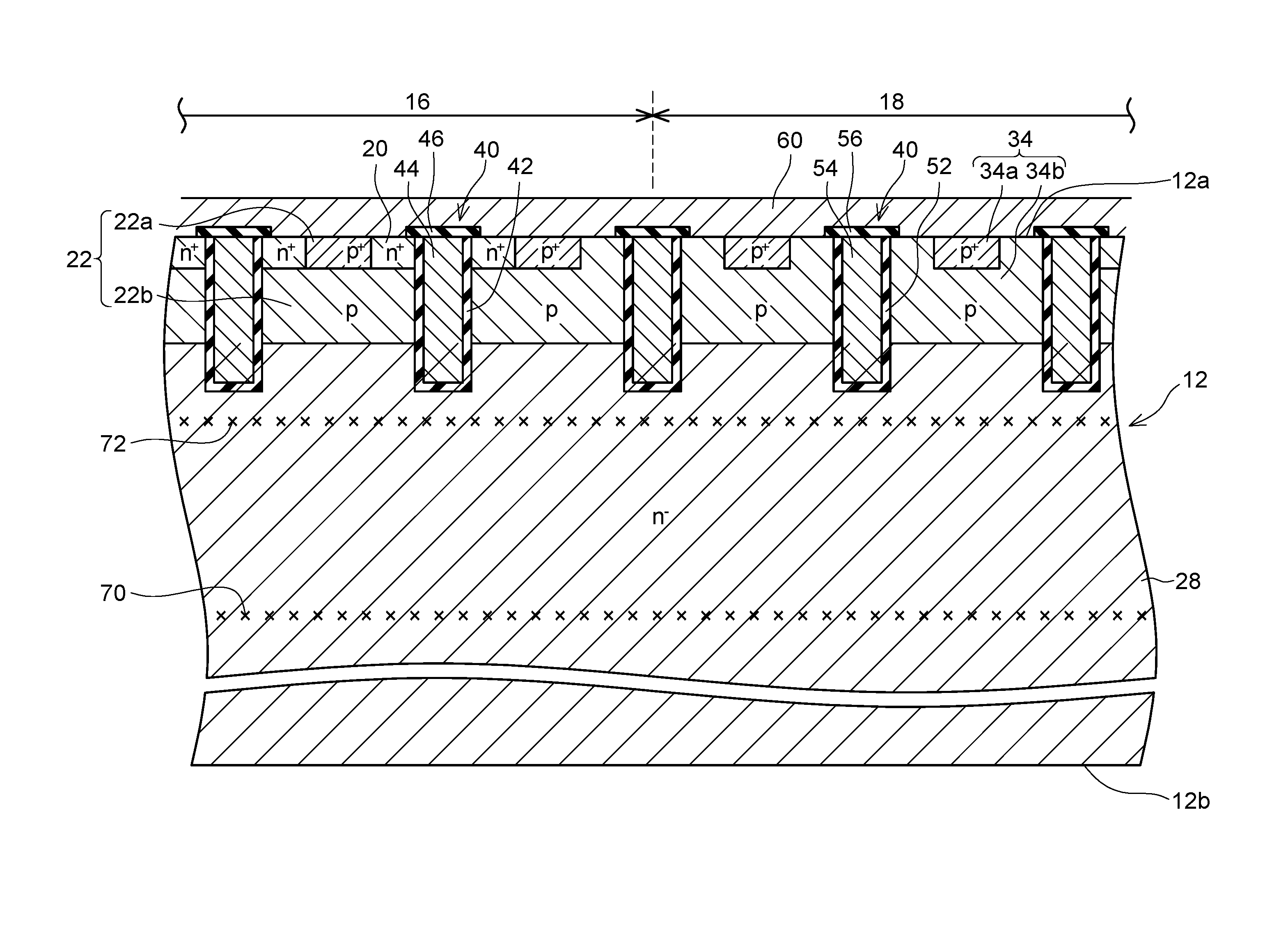
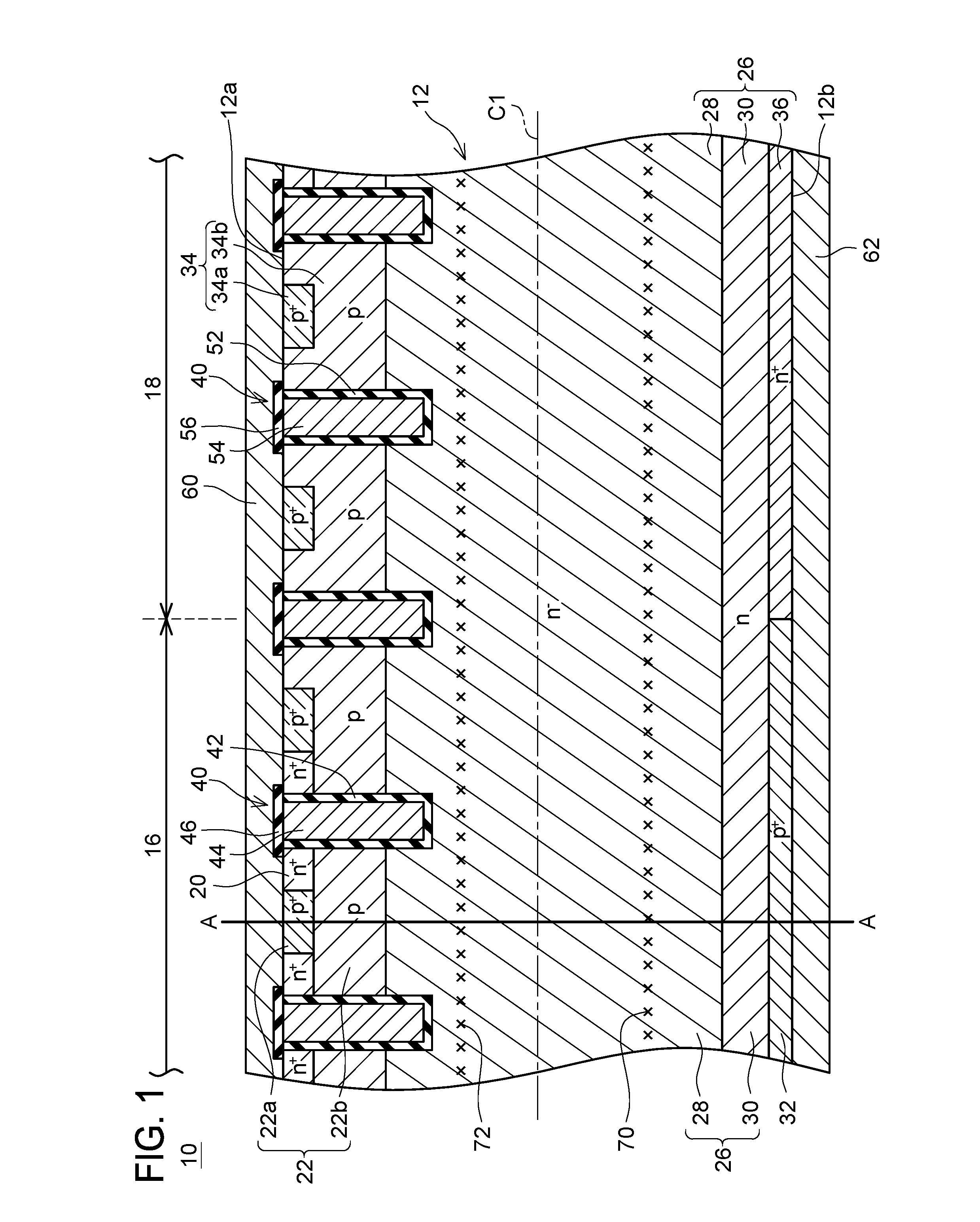
[0021]FIG. 1 shows a semiconductor device 10 that is manufactured by a method according to the present embodiment. The semiconductor device 10 includes a semiconductor substrate 12 and electrodes, insulators, and the like formed on a front surface 12 and a rear surface 12b of the semiconductor substrate 12. The semiconductor substrate 12 includes an IGBT region 16 in which an IGBT is formed and a diode region 18 in which a diode is formed. That is, the semiconductor device 10 is a so-called RC-IGBT.

[0022]The semiconductor substrate 12 is made of silicon. A plurality of trenches 40 is formed in the front surface 12a of the semiconductor substrate 12. The trenches 40 extend parallel to each other along a direction perpendicular to a paper plane of FIG. 1.

[0023]An inner surface of each trench 40 in the IGBT region 16 is covered with a gate insulating film 42. A gate electrode 44 is provided in an inner part of each trench 40 in the IGBT region 16. The gate electrode 44 is insulated fro...


PUM


Abstract

A semiconductor device includes a semiconductor substrate that includes an IGBT region. A first lifetime control layer extending along a planar direction of the semiconductor substrate is provided in a range in a drift region that is closer to the rear surface than an intermediate portion of the semiconductor substrate in a thickness direction. A crystal defect density in the first lifetime control layer is higher than any of a crystal defect density in a region adjacent to the first lifetime control layer on the rear surface side and a crystal defect density in a region adjacent to the first lifetime control layer on a front surface side. A crystal defect density in a region between the first lifetime control layer and the rear surface is lower than a crystal defect density in a region between the first lifetime control layer and the front surface.

Description

CROSS-REFERENCE TO RELATED APPLICATION[0001]This application claims priority to Japanese Patent Application No. 2015-037964 filed on Feb. 27, 2015, the entire contents of which are hereby incorporated by reference into the present application.TECHNICAL FIELD[0002]The technology disclosed herein relates to a semiconductor device and a method for manufacturing a semiconductor device.DESCRIPTION OF RELATED ART[0003]Japanese Patent Application Publication No, 2012-43891 A discloses a semiconductor device including an IGBT (Insulated Gate Bipolar Transistor) region. A lifetime control layer in which a crystal defect density is high is provided in a part of a drift region in the IGBT region. The lifetime control layer is formed in a range in the drift region that is closer to a rear surface than an intermediate portion of the semiconductor substrate in a thickness direction (i.e., in a range that is located near a collector region) of the semiconductor substrate. Such formation of the lif...

Claims


Application Information

Patent Timeline
Patent Type & Authority Applications(United States)
IPC IPC(8): H01L29/739H01L29/10H01L29/32H01L29/861H01L29/66H01L27/06H01L21/8234H01L29/08H01L21/265
CPCH01L29/7397H01L29/0804H01L29/1095H01L29/0821H01L29/32H01L29/861H01L29/66348H01L27/0635H01L21/8234H01L29/6609H01L21/26513H01L29/0834H01L29/8611H01L21/263H01L21/26506H01L27/0727H01L29/8613H01L29/407
Inventor KAMEYAMA, SATORUIWASAKI, SHINYA
Owner TOYOTA JIDOSHA KK
Why Eureka
Try Eureka